
Datasheet


Philips Semiconductors Product data
CBT3125Quadruple FET bus switch
2
2001 Dec 12 853-2309 27452
DESCRIPTION
The CBT3125 quadruple FET bus switch features independent line
switches. Each switch is disabled when the associated Output
Enable (OE
) input is HIGH.
FEATURES
• Standard ’125-type pinout (D, DB, and PW packages)
• 5 Ω switch connection between two ports
• TTL-compatible input levels
• Latch-up testing is done to JESDEC Standard JESD78 which
exceeds 500 mA
• ESD protection exceeds 2000 V HBM per JESD22-A114,
200 V MM per JESD22-A115, and 1000 V CDM per
JESD22-C101
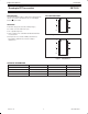
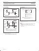
PIN CONFIGURATION
1
2
3
4
5
6
78
9
10
11
12
13
141OE
1A
1B
2OE
2A
2B
GND
V
CC
4OE
4A
4B
3OE
3A
3B
SA00562
Figure 1. SO14, SSOP14, and TSSOP14
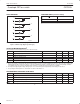
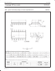
1
2
3
4
5
6
7
89
10
11
12
13
14
15
16NC
1OE
1A
1B
2OE
2A
2B
GND
V
CC
4OE
4A
4B
3OE
3A
3B
NC
SA00563
NC = no internal connection
Figure 2. SSOP(QSOP)16
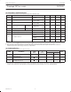
ORDERING INFORMATION
PACKAGES TEMPERATURE RANGE ORDER CODE DRAWING NUMBER
14-Pin Plastic SO –40 to +85 °C CBT3125D SOT108-1
14-Pin Plastic SSOP –40 to +85 °C CBT3125DB SOT337-1
16-Pin Plastic SSOP(QSOP) –40 to +85 °C CBT3125DS SOT519-1
14-Pin Plastic TSSOP –40 to +85 °C CBT3125PW SOT402-1
Standard packing quantities and other packaging data is available at www.philipslogic.com/packaging.