
Datasheet


Philips Semiconductors Product data
CBT3125Quadruple FET bus switch
2001 Dec 12
3
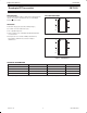
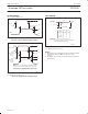
LOGIC DIAGRAM
1B
2B
3B
4B
3
6
8
11
2
5
9
12
1A
2A
3A
4A
1
4
10
13
1OE
2OE
3OE
4OE
SA00564
Pin numbers shown are for 14-pin package-types.
Figure 3. CBT3125 logic diagram (positive logic)
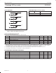
FUNCTION TABLE (each bus switch)
INPUT
OE
FUNCTION
L A = B
H disconnect
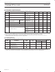
ABSOLUTE MAXIMUM RATINGS
1
Over operating free-air temperature range, unless otherwise noted.
SYMBOL
PARAMETER CONDITIONS MIN. MAX. UNIT
V
CC
supply voltage range –0.5 7 V
V
I
input voltage range see Note 2 –0.5 7 V
continuous channel current — 128 mA
I
K
input clamp current V
I/O
< 0 — –50 mA
T
stg
storage temperature range –65 +150 °C
NOTES:
1. Stresses beyond those listed under “absolute maximum ratings” may cause permanent damage to the device. These are stress ratings only,
and functional operation of the device at these or any other conditions beyond those indicated under “recommended operating conditions”
is not implied. Exposure to absolute-maximum-rated conditions for extended periods may affect device reliability.
2. The input and output negative-voltage ratings may be exceeded if the input and output clamp-current ratings are observed.
3. The package thermal impedance is calculated in accordance with JESD 51-7.
RECOMMENDED OPERATING CONDITIONS
1
SYMBOL
PARAMETER CONDITIONS MIN. MAX. UNIT
V
CC
supply voltage 4.5 5.5 V
V
IH
high-level control input voltage 2 — V
V
IL
low-level control input voltage — 0.8 V
T
amb
operating ambient temperature in free-air –40 +85 °C
NOTE:
1. All unused control inputs of the device must be held at V
CC
or GND to ensure proper device operation.