
Datasheet


Philips Semiconductors Product data
CBT3125Quadruple FET bus switch
2001 Dec 12
4
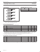
DC ELECTRICAL CHARACTERISTICS
Over recommended operating free-air temperature range, unless otherwise noted.
SYMBOL
PARAMETER CONDITIONS MIN. TYP.
1
MAX. UNIT
V
IK
Input clamp voltage
V
CC
= 4.5 V;
I
I
= –18 mA
— — –1.2 V
I
I
Input leakage current
V
CC
= 5.5 V;
V
I
= 5.5 V or GND
— — ±1 µA
I
CC
Quiescent supply current
V
CC
= 5.5 V; I
O
= 0;
V
I
= V
CC
or GND
— — 3 µA
∆I
CC
Additional supply current per
input pin (Note 2)
control inputs
V
CC
= 5.5 V;
one input at 3.4 V,
other inputs at V
CC
or GND
— — 2.5 mA
C
I
Input capacitance control inputs V
I
= 3 V or 0 — 1.7 — pF
C
IO(OFF)
Power-off leakage current V
O
= 3 V or 0; OE = V
CC
— 3.4 — pF
V
P
Pass gate voltage V
CC
= 5.0 V; V
I
= 5.0 V — 3.8 — V
V
CC
= 4.5 V; V
I
= 0 V;
I
I
= 64 mA
— 5 7 Ω
r
on
On-resistance (Note 3)
V
CC
= 4.5 V; V
I
= 0 V;
I
I
= 30 mA
— 5 7 Ω
V
CC
= 4.5 V; V
I
= 2.4 V;
I
I
= –15 mA
— 10 15 Ω
NOTES:
1. All typical values are at V
CC
= 5 V, unless otherwise noted. T
amb
= 25 °C.
2. This is the increase in supply current for each input that is at the specified TTL voltage level rather than V
CC
or GND.
3. Measured by the voltage drop between the A and the B terminals at the indicated current through the switch. On-state resistance is
determined by the lower of the voltages of the two (A or B) terminals.
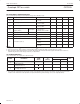
AC CHARACTERISTICS
T
amb
= –40 to +85 °C; C
L
= 50 pF, unless otherwise noted.
SYMBOL
PARAMETER
FROM TO
V
CC
= 5 V ± 0.5 V
UNIT
SYMBOL
PARAMETER
(INPUT) (OUTPUT)
Min Max
UNIT
t
pd
Propagation delay
1
A or B B or A — 0.25 ns
t
en
Output enable time
to High and Low level
OE A or B 1.0 5.4 ns
t
dis
Output disable time
from High and Low level
OE A or B 1 4.7 ns
NOTE:
1. This parameter is warranted but not production tested. The propagation delay is based on the RC time constant of the typical on-state
resistance of the switch and a load capacitance of 50 pF, when driven by an ideal voltage source (zero output impedance).