
Datasheet


Philips Semiconductors Product data
CBT3125Quadruple FET bus switch
2001 Dec 12
5
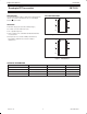
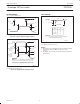
AC WAVEFORMS
V
M
= 1.5 V, V
IN
= GND to 3.0V
INPUT
1.5 V
OUTPUT
t
PLH
t
PHL
SA00028
1.5 V
1.5 V 1.5 V
3 V
0 V
V
OH
V
OL
t
PLH
and t
PHL
are the same as t
pd
.
Waveform 1. Input to Output Propagation Delays
Output Control
1.5 V
t
PZH
t
PHZ
V
OH
V
OL
t
PZL
t
PLZ
3.5 V
0 V
V
OL
+ 0.3 V
V
OH
– 0.3 V
SA00558
1.5 V
1.5 V 1.5 V
0 V
3 V
Output
Waveform 1
S1 at 7 V
(see Note)
Note:
Waveform 1 is for an output with internal conditions such that
the output is low except when disabled by the output control.
Waveform 2 is for an output with internal conditions such that
the output is high except when disabled by the output control.
Output
Waveform 2
S1 at Open
(see Note)
t
PLZ
and t
PHZ
are the same as t
dis
.
t
PZL
and t
PZH
are the same as t
en
.
Waveform 2. Output Enable and Disable Times
TEST CIRCUIT
C
L
= 50 pF
500 Ω
Load Circuit
DEFINITIONS
C
L
= Load capacitance includes jig and probe capacitance;
see AC CHARACTERISTICS for value.
TEST S1
t
pd
open
t
PLZ
/t
PZL
7 V
t
PHZ
/t
PZH
open
SA00012
500 Ω
From Output
Under Test
S1
7 V
Open
GND
t
PLZ
and t
PHZ
are the same as t
dis
.
t
PZL
and t
PZH
are the same as t
en
.
NOTES:
1. All input pulses are supplied by generators having the following
characteristics: PRR ≤ 10 MHz, Z
O
= 50 Ω, t
r
≤ 2.5 ns,
t
f
≤ 2.5 ns.
2. The outputs are measured one at a time with one transition per
measurement.