
Datasheet


CBT3257A All information provided in this document is subject to legal disclaimers. © NXP B.V. 2013. All rights reserved.
Product data sheet Rev. 5 — 4 April 2013 4 of 17
NXP Semiconductors
CBT3257A
Quad 1-of-2 multiplexer/demultiplexer
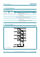
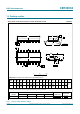
5.2 Pin description
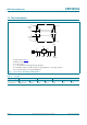
6. Functional description
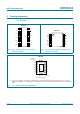
7. Limiting values
[1] The input and output negative voltage ratings may be exceeded if the input and output clamp current ratings are observed.
[2] For SO16 package: P
tot
derates linearly with 8 mW/K above 70 C.
[3] For SSOP16 and TSSOP16 package: P
tot
derates linearly with 5.5 mW/K above 70 C.
[4] For DHVQFN16 package: P
tot
derates linearly with 4.5 mW/K above 70 C.
Table 2. Pin description
Symbol Pin Description
S 1 select control input
1B1, 2B1, 3B1, 4B1, 2, 5, 11, 14 B1 outputs/inputs
1B2, 2B2, 3B2, 4B2 3, 6, 10, 13 B2 outputs/inputs
1A, 2A, 3A, 4A 4, 7, 9, 12 A inputs/outputs
GND 8 ground (0 V)
OE
15 output enable (active LOW)
V
CC
16 positive supply voltage
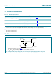
Table 3. Function selection
H = HIGH voltage level; L = LOW voltage level; X = Don’t care.
Inputs Switch
OE S
LLnA to nB1
L H nA to nB2
H X switch off
Table 4. Limiting values
In accordance with the Absolute Maximum Rating System (IEC 60134).
Symbol Parameter Conditions Min Max Unit
V
CC
supply voltage 0.5 +7.0 V
V
I
input voltage
[1]
0.5 +7.0 V
I
SW
switch current continuous current through each switch - 128 mA
I
IK
input clamping current V
I
<0V 50 mA
T
stg
storage temperature 65 +150 C
P
tot
total power dissipation T
amb
= 40 C to +85 C
SO16 package
[2]
-500mW
SSOP16 package
[3]
-500mW
TSSOP16 package
[3]
-500mW
DHVQFN16 package
[4]
-500mW