
Datasheet


CBT3257A All information provided in this document is subject to legal disclaimers. © NXP B.V. 2013. All rights reserved.
Product data sheet Rev. 5 — 4 April 2013 5 of 17
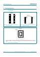
NXP Semiconductors
CBT3257A
Quad 1-of-2 multiplexer/demultiplexer
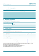
8. Recommended operating conditions
9. Static characteristics
[1] All typical values are measured at V
CC
=5V; T
amb
=25C.
[2] This is the increase in supply current for each input that is at the specified TTL voltage level rather than V
CC
or GND.
[3] Measured by the voltage drop between the nA and the nBn terminals at the indicated current through the switch. The lowest voltage of
the two (nA or nBn) terminals determines the ON resistance.
Table 5. Operating conditions
All unused control inputs of the device must be held at V
CC
or GND to ensure proper device operation.
Symbol Parameter Conditions Min Max Unit
V
CC
supply voltage 4.5 5.5 V
V
IH
HIGH-level input voltage 2.0 - V
V
IL
LOW-level input voltage - 0.8 V
T
amb
ambient temperature operating in free-air 40 +85 C
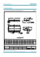
Table 6. Static characteristics
T
amb
=
40
Cto+85
C.
Symbol Parameter Conditions Min Typ
[1]
Max Unit
V
IK
input clamping voltage V
CC
=4.5V; I
I
= 18 mA - - 1.2 V
V
pass
pass voltage V
I
=V
CC
= 5.0 V; I
O
= 100 A 3.6 3.9 4.2 V
I
I
input leakage current V
CC
=5.5V; V
I
= GND or 5.5 V - - 1 A
I
CC
supply current V
CC
=5.5V; I
O
=0mA;
V
I
=V
CC
or GND
--3A
I
CC
additional supply current per input; V
CC
= 5.5 V; one input at
3.4 V, other inputs at V
CC
or GND
[2]
--2.5mA
C
I
input capacitance control pins; V
I
=3V or 0V -3.3-pF
C
io(off)
off-state input/output capacitance A port; V
O
= 3 V or 0 V; OE =V
CC
-9.9-pF
B port; V
O
= 3 V or 0 V; OE =V
CC
-6.4-pF
R
ON
ON resistance V
CC
=4.5V
[3]
V
I
=0V; I
I
=64mA - 5 7
V
I
=0V; I
I
=30mA - 5 7
V
I
= 2.4 V; I
I
=15mA - 10 15