
Datasheet
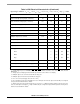

Flash Memory Characteristics
56F803 Technical Data, Rev. 16
Freescale Semiconductor 25
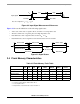
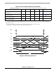
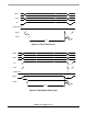
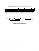
Figure 3-4 Flash Program Cycle
Cumulative program
HV period
2
Thv
–3–ms Figure 3-4
Program hold time
3
Tpgh
––– Figure 3-4
Address/data set up time
3
Tads
––– Figure 3-4
Address/data hold time
3
Tadh
––– Figure 3-4
1. One cycle is equal to an erase program and read.
2. Thv is the cumulative high voltage programming time to the same row before next erase. The same address cannot be programmed
twice before next erase.
3. Parameters are guaranteed by design in smart programming mode and must be one cycle or greater.
*The Flash interface unit provides registers for the control of these parameters.
Table 3-7 Flash Timing Parameters (Continued)
Operating Conditions: V
SS
= V
SSA
= 0 V, V
DD
= V
DDA
= 3.0–3.6V, T
A
= –40° to +85°C, C
L
≤ 50pF
Characteristic Symbol Min Typ Max Unit Figure
XADR
YADR
YE
DIN
PROG
NVSTR
Tnvs
Tpgs
Tadh
Tprog
Tads
Tpgh
Tnvh
Trcv
Thv
IFREN
XE