
Datasheet

Signals and Package Information
56F826 Technical Data, Rev. 14
Freescale Semiconductor 13
RD
26 Output Read Enable—RD is asserted during external memory read cycles. When RD is
asserted low, pins D0–D15 become inputs and an external device is enabled
onto the device data bus. When RD
is deasserted high, the external data is
latched inside the device. When RD is asserted, it qualifies the A0–A15, PS, and
DS
pins. RD can be connected directly to the OE pin of a Static RAM or ROM.
WR
27 Output Write Enable—WR is asserted during external memory write cycles. When WR
is asserted low, pins D0–D15 become outputs and the device puts data on the
bus. When WR
is deasserted high, the external data is latched inside the
external device. When WR is asserted, it qualifies the A0–A15, PS, and DS pins.
WR can be connected directly to the WE pin of a Static RAM.
TA0
(GPIOF0)
91 Input/Output
Input/Output
TA0–3—Timer A Channels 0, 1, 2, and 3
Port F GPIO—These four General Purpose I/O (GPIO) pins can be individually
programmed as input or output.
After reset, the default state is Quad Timer.
TA1
(GPIOF1)
90
TA2
(GPIOF2)
89
TA3
(GPIOF3)
88
TCK 100 Input
(Schmitt)
Test Clock Input—This input pin provides a gated clock to synchronize the test
logic and shift serial data to the JTAG/OnCE port. The pin is connected internally
to a pull-down resistor.
TMS 1 Input
(Schmitt)
Test Mode Select Input—This input pin is used to sequence the JTAG TAP
controller’s state machine. It is sampled on the rising edge of TCK and has an
on-chip pull-up resistor.
Note: Always tie the TMS pin to V
DD
through a 2.2K resistor.
TDI 2 Input
(Schmitt)
Test Data Input—This input pin provides a serial input data stream to the
JTAG/OnCE port. It is sampled on the rising edge of TCK and has an on-chip
pull-up resistor.
TDO 3 Output Test Data Output—This tri-statable output pin provides a serial output data
stream from the JTAG/OnCE port. It is driven in the Shift-IR and Shift-DR
controller states, and changes on the falling edge of TCK.
TRST
4 Input
(Schmitt)
Test Reset—As an input, a low signal on this pin provides a reset signal to the
JTAG TAP controller. To ensure complete hardware reset, TRST should be
asserted whenever RESET
is asserted. The only exception occurs in a
debugging environment when a hardware device reset is required and it is
necessary not to reset the JTAG/OnCE module. In this case, assert RESET
, but
do not assert TRST
. TRST must always be asserted at power-up.
Note: For normal operation, connect TRST
directly to V
SS
. If the design is to be used
in a debugging environment, TRST
may be tied to V
SS
through a 1K resistor.
DE
98 Output Debug Event—DE provides a low pulse on recognized debug events.
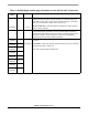
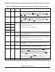
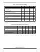
Table 2-1 56F826 Signal and Package Information for the 100 Pin LQFP (Continued)
Signal
Name
Pin No. Type Description