
Datasheet


56F826 Technical Data, Rev. 14
30 Freescale Semiconductor
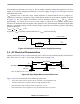
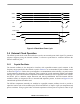
3.6.3 External Clock Source
The recommended method of connecting an external clock is given in Figure 3-11. The external clock
source is connected to XTAL and the EXTAL pin is held V
DDA
/2.
Figure 3-11 Connecting an External Clock Signal
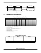
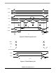
Figure 3-12 External Clock Timing
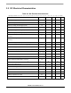
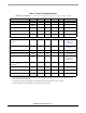
Table 3-8 External Clock Operation Timing Requirements
Operating Conditions: V
SSIO
=V
SS
= V
SSA
= 0V, V
DDA
=V
DDIO
=3.0–3.6V, V
DD
= 2.25–2.75V, T
A
= –40° to +85°C, C
L
≤ 50pF, f
op
= 80MHz
Characteristic Symbol Min Typ Max Unit
Frequency of operation (external clock driver)
1
1. See Figure 3-11 for details on using the recommended connection of an external clock driver.
f
osc
04
80
2
2. When using Time of Day (TOD), maximum external frequency is 6MHz.
MHz
Clock Pulse Width
3,
4
3. The high or low pulse width must be no smaller than 6.25ns or the chip will not function.
4. Parameters listed are guaranteed by design.
t
PW
6.25 — — ns
56F826
XTAL
EXTAL
External
V
DDA
/2
Clock
External
Clock
V
IH
V
IL
Note: The midpoint is V
IL
+ (V
IH
– V
IL
)/2.
90%
50%
10%
90%
50%
10%
t
PW
t
PW