
Datasheet


GTL2002 All information provided in this document is subject to legal disclaimers. © NXP B.V. 2013. All rights reserved.
Product data sheet Rev. 8 — 19 August 2013 9 of 27
NXP Semiconductors
GTL2002
2-bit bidirectional low voltage translator
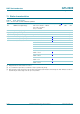
11. Static characteristics
[1] All typical values are measured at T
amb
=25C.
[2] C
io(on)
maximum of 30 pF and C
io(off)
maximum of 15 pF is guaranteed by design.
[3] Measured by the voltage drop between the Sn and the Dn terminals at the indicated current through the switch. ON-state resistance is
determined by the lowest voltage of the two (Sn or Dn) terminals.
Table 9. Static characteristics
T
amb
=
40
C to +85
C, unless otherwise specified.
Symbol Parameter Conditions Min Typ
[1]
Max Unit
V
OL
LOW-level output voltage V
DD
= 3.0 V; V
SREF
= 1.365 V;
V
Sn
or V
Dn
= 0.175 V;
I
clamp
= 15.2 mA
- 260 350 mV
V
IK
input clamping voltage I
I
= 18 mA; V
GREF
=0V - - 1.2 V
I
LI(gate)
gate input leakage current V
I
=5V; V
GREF
=0V --5A
C
ig
input capacitance at gate pin GREF; V
I
= 3 V or 0 V - 19.4 - pF
C
io(off)
off-state input/output capacitance V
O
= 3 V or 0 V; V
GREF
=0V
[2]
-7.4-pF
C
io(on)
on-state input/output capacitance V
O
= 3 V or 0 V; V
GREF
=3V
[2]
-18.6-pF
R
on
ON-state resistance V
I
=0V; I
O
=64mA
[3]
V
GREF
=4.5V - 3.5 5
V
GREF
=3V - 4.4 7
V
GREF
=2.3V - 5.5 9
V
GREF
=1.5V - 67 105
V
I
=0V; I
O
=30mA;
V
GREF
=1.5V
[3]
-915
V
I
=2.4V; I
O
=15mA;
V
GREF
=4.5V
[3]
-710
V
I
=2.4V; I
O
=15mA;
V
GREF
=3V
[3]
-5880
V
I
=1.7V; I
O
=15mA;
V
GREF
=2.3V
[3]
-5070