
Datasheet


HEF4011B All information provided in this document is subject to legal disclaimers. © NXP B.V. 2011. All rights reserved.
Product data sheet Rev. 5 — 21 November 2011 2 of 12
NXP Semiconductors
HEF4011B
Quad 2-input NAND gate
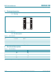
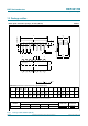
5. Pinning information
5.1 Pinning
5.2 Pin description
6. Functional description
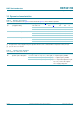
[1] H = HIGH voltage level; L = LOW voltage level.
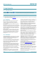
Fig 3. Pin configuration
HEF4011B
1A V
DD
1B 4B
1Y 4A
2Y 4Y
2A 3Y
2B 3B
V
SS
3A
001aan876
1
2
3
4
5
6
7 8
10
9
12
11
14
13
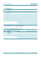
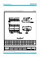
Table 2. Pin description
Symbol Pin Description
nA 1, 5, 8, 12 input
nB 2, 6, 9, 13 input
nY 3, 4, 10, 11 output
V
SS
7 ground (0 V)
V
DD
14 supply voltage
Table 3. Function table
[1]
Input Output
nA nB nY
LLH
LHH
HL H
HHL