
Datasheet


HEF4011B All information provided in this document is subject to legal disclaimers. © NXP B.V. 2011. All rights reserved.
Product data sheet Rev. 5 — 21 November 2011 4 of 12
NXP Semiconductors
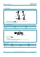
HEF4011B
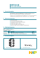
Quad 2-input NAND gate
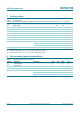
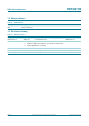
9. Static characteristics
Table 6. Static characteristics
V
SS
= 0 V; V
I
=V
SS
or V
DD
; unless otherwise specified.
Symbol Parameter Conditions V
DD
T
amb
= 40 C T
amb
= +25 C T
amb
= +85 C T
amb
= +125 C Unit
Min Max Min Max Min Max Min Max
V
IH
HIGH-level
input voltage
I
O
< 1 A 5 V 3.5 - 3.5 - 3.5 - 3.5 - V
10 V7.0-7.0-7.0- 7.0 -V
15 V 11.0 - 11.0 - 11.0 - 11.0 - V
V
IL
LOW-level
input voltage
I
O
< 1 A 5 V - 1.5 - 1.5 - 1.5 - 1.5 V
10 V - 3.0 - 3.0 - 3.0 - 3.0 V
15 V - 4.0 - 4.0 - 4.0 - 4.0 V
V
OH
HIGH-level
output voltage
I
O
< 1 A 5 V 4.95 - 4.95 - 4.95 - 4.95 - V
10 V 9.95 - 9.95 - 9.95 - 9.95 - V
15 V 14.95 - 14.95 - 14.95 - 14.95 - V
V
OL
LOW-level
output voltage
I
O
< 1 A 5 V - 0.05 - 0.05 - 0.05 - 0.05 V
10 V - 0.05 - 0.05 - 0.05 - 0.05 V
15 V - 0.05 - 0.05 - 0.05 - 0.05 V
I
OH
HIGH-level
output current
V
O
= 2.5 V 5 V - 1.7 - 1.4 - 1.1 - 1.1 mA
V
O
= 4.6 V 5 V - 0.64 - 0.5 - 0.36 - 0.36 mA
V
O
= 9.5 V 10 V - 1.6 - 1.3 - 0.9 - 0.9 mA
V
O
= 13.5 V 15 V - 4.2 - 3.4 - 2.4 - 2.4 mA
I
OL
LOW-level
output current
V
O
= 0.4 V 5 V 0.64 - 0.5 - 0.36 - 0.36 - mA
V
O
= 0.5 V 10 V 1.6 - 1.3 - 0.9 - 0.9 - mA
V
O
= 1.5 V 15 V 4.2 - 3.4 - 2.4 - 2.4 - mA
I
I
input leakage
current
15 V - 0.1 - 0.1 - 1.0 - 1.0 A
I
DD
supply current all valid input
combinations;
I
O
=0A
5 V - 0.25 - 0.25 - 7.5 - 7.5 A
10 V - 0.5 - 0.5 - 15.0 - 15.0 A
15 V - 1.0 - 1.0 - 30.0 - 30.0 A
C
I
input
capacitance
---7.5-- - -pF