
Datasheet


HEF4011B All information provided in this document is subject to legal disclaimers. © NXP B.V. 2011. All rights reserved.
Product data sheet Rev. 5 — 21 November 2011 5 of 12
NXP Semiconductors
HEF4011B
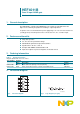
Quad 2-input NAND gate
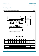
10. Dynamic characteristics
[1] The typical value of the propagation delay and output transition time can be calculated with the extrapolation formula (C
L
in pF).
[2] t
pd
is the same as t
PLH
and t
PHL
.
Table 7. Dynamic characteristics
T
amb
= 25
C; for waveforms see Figure 4; for test circuit see Figure 5; unless otherwise specified.
Symbol Parameter Extrapolation formula
[1]
V
DD
Min Typ Max Unit
t
pd
propagation delay 28 + 0.55 C
L
5 V
[2]
- 55 110 ns
14 + 0.23 C
L
10 V - 25 45 ns
12 + 0.16 C
L
15 V - 20 35 ns
t
THL
HIGH to LOW output transition time 10 + 1.00 C
L
5 V - 60 120 ns
9 + 0.42 C
L
10 V - 30 60 ns
6 + 0.28 C
L
15 V - 20 40 ns
t
TLH
LOW to HIGH output transition time 10 + 1.00 C
L
5 V - 60 120 ns
9 + 0.42 C
L
10 V - 30 60 ns
6 + 0.28 C
L
15 V - 20 40 ns
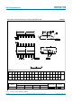
Table 8. Dynamic power dissipation
V
SS
= 0 V; t
r
= t
f
20 ns; T
amb
= 25
C.
Symbol Parameter V
DD
Typical formula Where
P
D
dynamic power dissipation 5 V P
D
= 1300 f
i
+ (f
o
C
L
) V
DD
2
(W) f
i
= input frequency in MHz;
f
o
= output frequency in MHz;
C
L
= output load capacitance in pF;
(f
o
C
L
) = sum of the outputs;
V
DD
= supply voltage in V.
10 V P
D
= 6000 f
i
+ (f
o
C
L
) V
DD
2
(W)
15 V P
D
= 20100 f
i
+ (f
o
C
L
) V
DD
2
(W)