
Datasheet


HEF4011B All information provided in this document is subject to legal disclaimers. © NXP B.V. 2011. All rights reserved.
Product data sheet Rev. 5 — 21 November 2011 6 of 12
NXP Semiconductors
HEF4011B
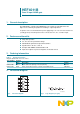
Quad 2-input NAND gate
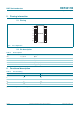
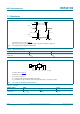
11. Waveforms
Measurement points are given in Table 9.
Logic levels: V
OL
and V
OH
are typical output voltage levels that occur with the output load.
Fig 4. Propagation delay, output transition time
001aag197
input
output
t
PLH
t
PHL
0 V
V
I
V
M
V
M
V
OH
V
OL
t
TLH
t
THL
90 %
10 %
10 %
90 %
t
r
t
f
Table 9. Measurement points
Supply voltage Input Output
V
DD
V
M
V
M
5 V to 15 V 0.5V
DD
0.5V
DD
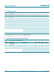
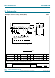
Test data is given in Table 10.
Definitions for test circuit:
DUT = Device Under Test.
C
L
= load capacitance including jig and probe capacitance.
R
T
= termination resistance should be equal to the output impedance Z
o
of the pulse generator.
Fig 5. Test circuit for measuring switching times
V
DD
V
I
V
O
001aag182
DUT
C
L
R
T
G
Table 10. Test data
Supply voltage Input Load
V
DD
V
I
t
r
, t
f
C
L
5 V to 15 V V
SS
or V
DD
20 ns 50 pF