
Datasheet


HEF4014B All information provided in this document is subject to legal disclaimers. © NXP B.V. 2011. All rights reserved.
Product data sheet Rev. 8 — 21 November 2011 4 of 14
NXP Semiconductors
HEF4014B
8-bit static shift register
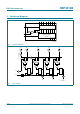
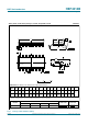
7. Functional description
[1] H = HIGH voltage level; L = LOW voltage level; X = don’t care; nD = HIGH or LOW;
= LOW-to-HIGH clock transition; = HIGH-to-LOW clock transition;
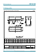
8. Limiting values
[1] For DIP16 package: P
tot
derates linearly with 12 mW/K above 70 C.
[2] For SO16 package: P
tot
derates linearly with 8 mW/K above 70 C.
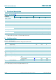
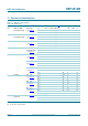
Table 3. Function table
[1]
Number of clock
transitions
Inputs Outputs
CP DS PE Q5 Q6 Q7
Serial operation
1 1DLXXX
2 2DLXXX
3 3DLXXX
6 XL1DXX
7 XL2D1DX
8 X L 3D 2D 1D
X X no change no change no change
Parallel operation
1 X H D5 D6 D7
X X no change no change no change
Table 4. Limiting values
In accordance with the Absolute Maximum Rating System (IEC 60134).
Symbol Parameter Conditions Min Max Unit
V
DD
supply voltage 0.5 +18 V
I
IK
input clamping current V
I
< 0.5 V or V
I
>V
DD
+ 0.5 V - 10 mA
V
I
input voltage 0.5 V
DD
+ 0.5 V
I
OK
output clamping current V
O
< 0.5 V or V
O
>V
DD
+ 0.5 V - 10 mA
I
I/O
input/output current - 10 mA
I
DD
supply current - 50 mA
T
stg
storage temperature 65 +150 C
T
amb
ambient temperature 40 +85 C
P
tot
total power dissipation T
amb
= 40 C to +85 C
DIP16 package
[1]
- 750 mW
SO16 package
[2]
- 500 mW
P power dissipation per output - 100 mW