
Datasheet


HEF4014B All information provided in this document is subject to legal disclaimers. © NXP B.V. 2011. All rights reserved.
Product data sheet Rev. 8 — 21 November 2011 7 of 14
NXP Semiconductors
HEF4014B
8-bit static shift register
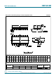
12. Waveforms
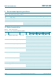
Table 8. Dynamic power dissipation P
D
P
D
can be calculated from the formulas shown. V
SS
= 0 V; t
r
= t
f
20 ns; T
amb
= 25
C.
Symbol Parameter V
DD
Typical formula for P
D
(W) Where:
P
D
dynamic power
dissipation
5V P
D
= 900 f
i
+ (f
o
C
L
) V
DD
2
f
i
= input frequency in MHz;
f
o
= output frequency in MHz;
C
L
= output load capacitance in pF;
V
DD
= supply voltage in V;
(C
L
f
o
) = sum of the outputs.
10 V P
D
= 4300 f
i
+ (f
o
C
L
) V
DD
2
15 V P
D
= 12000 f
i
+ (f
o
C
L
) V
DD
2
Measurement points are given in Table 9.
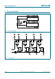
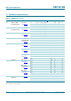
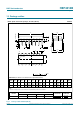
Fig 4. CP to Qn propagation delays and output transition times
The shaded areas indicate where change is permitted for predictable output performance.
Set-up and hold times are shown as positive values but may be specified as negative values.
Measurement points are given in Table 9
.
Fig 5. Minimum clock pulse width, and set-up and hold times for PE to CP, DS to CP, and D to CP
001aaj456
t
PHL
t
t
t
t
CP input
Qn output
V
I
V
SS
V
M
V
OH
V
OL
V
M
90 %
10 %
t
PLH
001aae559
CP input
V
I
V
SS
V
I
V
SS
V
I
V
SS
V
I
V
SS
D input
PE input
DS input
t
W
t
h
t
su
50 %
50 %
50 % 50 % 50 %
f
clk(max)
t
r
t
f
t
h
t
h
t
su
t
su
50 % 50 %
t
h
t
su
50 %
50 %
50 %
50 %
50 %