
Datasheet


HEF4030B All information provided in this document is subject to legal disclaimers. © NXP B.V. 2013. All rights reserved.
Product data sheet Rev. 4 — 13 November 2013 2 of 12
NXP Semiconductors
HEF4030B
Quad 2-input EXCLUSIVE-OR gate
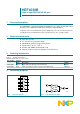
5. Pinning information
5.1 Pinning
5.2 Pin description
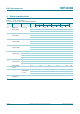
6. Functional description
[1] H = HIGH voltage level; L = LOW voltage level
Fig 3. Pin configuration
+()%
$
9
''
%
%
<
$
<
<
$
<
%
%
9
6
6
$
DDD
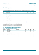
Table 2. Pin description
Symbol Pin Description
1A, 2A, 3A, 4A 1, 5, 8, 12 data input
1B, 2B, 3B, 4B 2, 6, 9, 13 data input
1Y, 2Y, 3Y, 4Y 3, 4, 10, 11 data output
V
SS
7 ground (0 V)
V
DD
14 supply voltage
Table 3. Functional table
[1]
Input Output
nA nB nY
LLL
LHH
HL H
HHL