
Datasheet


HEF4030B All information provided in this document is subject to legal disclaimers. © NXP B.V. 2013. All rights reserved.
Product data sheet Rev. 4 — 13 November 2013 3 of 12
NXP Semiconductors
HEF4030B
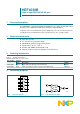
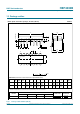
Quad 2-input EXCLUSIVE-OR gate
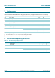
7. Limiting values
[1] For DIP14 packages: above T
amb
= 70 C, P
tot
derates linearly with 12 mW/K.
[2] For SO14 packages: above T
amb
= 70 C, P
tot
derates linearly with 8 mW/K.
8. Recommended operating conditions
Table 4. Limiting values
In accordance with the Absolute Maximum Rating System (IEC 60134). Voltages are referenced to V
SS
= 0 V (ground).
Symbol Parameter Conditions Min Max Unit
V
DD
supply voltage 0.5 +18 V
I
IK
input clamping current V
I
< 0.5 V or V
I
>V
DD
+ 0.5 V - 10 mA
V
I
input voltage 0.5 V
DD
+ 0.5 V
I
OK
output clamping current V
O
< 0.5 V or V
O
>V
DD
+ 0.5 V - 10 mA
I
I/O
input/output current - 10 mA
I
DD
supply current - 50 mA
T
stg
storage temperature 65 +150 C
T
amb
ambient temperature 40 +125 C
P
tot
total power dissipation T
amb
= 40 C to + 125 C
DIP14
[1]
-750mW
SO14
[2]
-500mW
P power dissipation per output - 100 mW
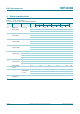
Table 5. Recommended operating conditions
Symbol Parameter Conditions Min Typ Max Unit
V
DD
supply voltage 3 - 15 V
V
I
input voltage 0 - V
DD
V
T
amb
ambient temperature in free air 40 - +125 C
t/V input transition rise and fall rate V
DD
= 5 V --3.75s/V
V
DD
= 10 V --0.5s/V
V
DD
= 15 V --0.08s/V