
Datasheet

HEF4794B All information provided in this document is subject to legal disclaimers. © NXP B.V. 2011. All rights reserved.
Product data sheet Rev. 7 — 16 November 2011 10 of 18
NXP Semiconductors
HEF4794B
8-stage shift-and-store register LED driver
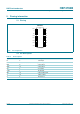
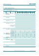
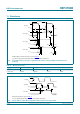
Measurement points are given in Table 9.
V
OL
is the typical output voltage level that occurs with the output load.
Fig 8. Enable and disable times for input OE
001aag803
OE input
output
LOW to OFF-state
OFF-state to LOW
V
I
V
M
V
X
t
PZL
t
PLZ
outputs
disabled
outputs
enabled
outputs
enabled
V
Y
V
SS
V
DD
V
OL
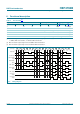
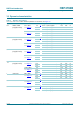
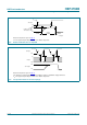
Measurement points are given in Table 9.
The shaded areas indicate when the input is permitted to change for predictable output performance.
V
OL
is the typical output voltage level that occurs with the output load.
Fig 9. Set-up and hold times for the data input (D)
V
I
V
M
t
su
t
h
t
su
t
h
V
M
V
SS
V
I
V
SS
V
DD
CP input
D input
QPn output
001aag805
V
OL