:/ &6 3 IP4085CX4; IP4385CX4; IP4386CX4; IP4387CX4 Integrated high-performance ESD protection diodes Rev. 2 — 14 December 2012 Product data sheet 1. Product profile 1.1 General description Integrated high-performance protection diodes protecting appliances against ElectroStatic Discharge (ESD) of 30 kV, far exceeding IEC 61000-4-2 level 4 standard, overvoltage and wrong polarity. Each device includes one high-level ESD protection diode in a 4-channel 0.4 mm (IP438xCX4) or 0.
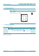
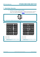
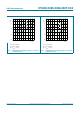
IP4085/4385/4386/4387/CX4 NXP Semiconductors Integrated high-performance ESD protection diodes 2. Pinning information Table 1. Pin Pinning Description Simplified outline Graphic symbol A1 and A2 cathode B1 and B2 anode A1 bump A1 index area 1 2 B1 A2 B2 006aad220 A B 008aaa236 transparent top view, solder balls facing down 3. Ordering information Table 2.
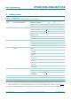
IP4085/4385/4386/4387/CX4 NXP Semiconductors Integrated high-performance ESD protection diodes 4. Limiting values Table 3. Limiting values In accordance with the Absolute Maximum Rating System (IEC 60134). Symbol Parameter Conditions Min Max Unit VRWM reverse standoff voltage IP4085CX4; IP4386CX4 0.5 +14 V IP4385CX4 0.5 +5.5 V IP4387CX4 0.5 +8.
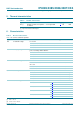
IP4085/4385/4386/4387/CX4 NXP Semiconductors Integrated high-performance ESD protection diodes 5. Thermal characteristics Table 4. Symbol Rth(j-a) [1] Thermal characteristics Parameter thermal resistance from junction to ambient Conditions [1] on a 2-layer PCB Typ Unit 130 K/W Depends on details of PCB layout. 6. Characteristics Table 5. Electrical characteristics Tamb = 25 C; unless otherwise specified.
IP4085/4385/4386/4387/CX4 NXP Semiconductors Integrated high-performance ESD protection diodes 7. Application information 7.1 Forward current DC clamping voltage The forward current DC clamping voltage is an indicator of protection level of circuit from voltage sources with the wrong polarity. Figure 1 shows basic measurement setup. VCL IF V 006aad221 Fig 1. Measuring DC clamping voltage with forward current 001aaj241 1.1 VCL (V) 001aaj242 1.1 VCL (V) (1) 1.0 1.0 (1) (2) (2) 0.9 0.
IP4085/4385/4386/4387/CX4 NXP Semiconductors Integrated high-performance ESD protection diodes 001aaj243 1.1 VCL (V) VCL (V) (1) 1.0 001aaj244 1.1 (1) 1.0 (2) (2) (3) 0.9 0.9 (3) 0.8 0.8 0.7 0.7 0 0.2 0.4 0.6 0.8 1.0 0 0.2 IF (A) (1) Tamb = +25 C (2) Tamb = +85 C (2) Tamb = +85 C (3) Tamb = 30 C (3) Tamb = 30 C IP4386CX4: DC clamping voltage as a function of forward current 0.6 0.8 1.0 IF (A) (1) Tamb = +25 C Fig 4. 0.4 Fig 5.
IP4085/4385/4386/4387/CX4 NXP Semiconductors Integrated high-performance ESD protection diodes 7.2 Peak clamping voltage The peak clamping voltage for forward and reverse current pulses of 8/20 s (IEC 61000-4-5) is an indicator of protection level of circuits from power surges due to voltage discharges. The current pulse shape over time is shown in Figure 7. The basic measurement setup for forward current and reverse current pulses respectively are shown in Figure 6 and Figure 12.
IP4085/4385/4386/4387/CX4 NXP Semiconductors Integrated high-performance ESD protection diodes 006aad222 17 VCL (V) 006aad223 20 VCL (V) 15 (3) 16 (1) 13 (3) (2) 11 12 9 (1) (2) 8 7 20 28 36 44 20 28 36 IF (A) (1) Tamb = +25 C (1) Tamb = +25 C (2) Tamb = +85 C (2) Tamb = +85 C (3) Tamb = 30 C (3) Tamb = 30 C Fig 8. IP4085CX4: peak clamping voltage as a function of forward current 006aad224 20 (3) (2) (1) VCL (V) 44 IF (A) Fig 9.
IP4085/4385/4386/4387/CX4 NXP Semiconductors Integrated high-performance ESD protection diodes VCL V IPP 006aad226 Fig 12. Measuring peak clamping voltage with reverse current 006aad228 19 VCL (V) (2) VCL (V) 006aad229 8.75 8.50 (2) 18 8.25 (1) (1) 8.00 (3) 17 (3) 7.75 16 0.2 0.4 0.6 0.8 1.0 1.2 1.4 IR (A) 1.6 7.50 0.4 0.8 1.2 1.6 IR (A) (1) Tamb = +25 C (1) Tamb = +25 C (2) Tamb = +85 C (2) Tamb = +85 C (3) Tamb = 30 C (3) Tamb = 30 C Fig 13.
IP4085/4385/4386/4387/CX4 NXP Semiconductors Integrated high-performance ESD protection diodes 006aad230 19 VCL (V) 006aad231 12.2 (2) VCL (V) (2) 18 11.8 (1) (1) 17 11.4 (3) (3) 16 0.3 0.7 1.1 1.5 11.0 0.4 0.8 IR (A) 1.2 1.6 IR (A) (1) Tamb = +25 C. (1) Tamb = +25 C. (2) Tamb = +85 C. (2) Tamb = +85 C. (3) Tamb = 30 C. (3) Tamb = 30 C. Fig 15. IP4386CX4: peak clamping voltage as a function of reverse current Fig 16.
IP4085/4385/4386/4387/CX4 NXP Semiconductors Integrated high-performance ESD protection diodes 8. Package outline WLCSP4: wafer level chip-size package; 4 bumps (2 x 2) D bump A1 index area A2 A E A1 detail X e b B e A 1 2 X European projection wlcsp4_2x2_po Fig 17. Package outline WLCSP4 Table 6. Package outline dimensions of IP4085CX4 (WLCSP4) Symbol Min Typ Max Unit A 0.60 0.65 0.70 mm A1 0.22 0.24 0.26 mm A2 0.38 0.41 0.44 mm b 0.27 0.32 0.37 mm D 0.86 0.
IP4085/4385/4386/4387/CX4 NXP Semiconductors Integrated high-performance ESD protection diodes Table 7. Package outline dimensions of IP438xCX4 (WLCSP4) Symbol Min Typ Max Unit A 0.56 0.61 0.66 mm A1 0.18 0.20 0.22 mm A2 0.38 0.41 0.44 mm b 0.21 0.26 0.31 mm D 0.71 0.76 0.76 mm E 0.71 0.76 0.81 mm e 0.4 0.4 0.4 mm 9. Design and assembly recommendations 9.
IP4085/4385/4386/4387/CX4 NXP Semiconductors Integrated high-performance ESD protection diodes T (°C) Treflow(peak) 250 230 cooling rate 217 preheat t1 t (s) t2 t3 t4 t5 001aai943 The device is capable of withstanding at least three reflows of this profile. Fig 18. Pb-free solder reflow profile Table 10.
IP4085/4385/4386/4387/CX4 NXP Semiconductors Integrated high-performance ESD protection diodes 10. Soldering D e c (4×) e solder resist E solder paste = solderland f (4×) occupied area Dimensions in mm wlcsp4_2x2_fr Fig 19. Reflow soldering footprint WLCSP4 Table 11. Soldering dimensions of IP4085CX4 (WLCSP4) Symbol Min Typ Max Unit c - 0.31 - mm D 0.86 0.91 0.96 mm E 0.86 0.91 0.96 mm e - 0.5 - mm f - 0.385 - mm Table 12.
IP4085/4385/4386/4387/CX4 NXP Semiconductors Integrated high-performance ESD protection diodes 11. Revision history Table 13. Revision history Document ID Release date Data sheet status Change Supersedes notice IP4085_4385_4386_4387_CX4 v.2 20121214 Product data sheet - Modifications: IP4085_4385_4386_4387_CX4 v.1 • • • • • • • • • • • • IP4085_4385_4386_4387_CX4 v.
IP4085/4385/4386/4387/CX4 NXP Semiconductors Integrated high-performance ESD protection diodes 12. Legal information 12.1 Data sheet status Document status[1][2] Product status[3] Definition Objective [short] data sheet Development This document contains data from the objective specification for product development. Preliminary [short] data sheet Qualification This document contains data from the preliminary specification.
IP4085/4385/4386/4387/CX4 NXP Semiconductors Integrated high-performance ESD protection diodes Export control — This document as well as the item(s) described herein may be subject to export control regulations. Export might require a prior authorization from competent authorities. Quick reference data — The Quick reference data is an extract of the product data given in the Limiting values and Characteristics sections of this document, and as such is not complete, exhaustive or legally binding.
NXP Semiconductors IP4085/4385/4386/4387/CX4 Integrated high-performance ESD protection diodes 14. Contents 1 1.1 1.2 1.3 2 3 4 5 6 7 7.1 7.2 8 9 9.1 9.2 10 11 12 12.1 12.2 12.3 12.4 13 14 Product profile . . . . . . . . . . . . . . . . . . . . . . . . . . 1 General description . . . . . . . . . . . . . . . . . . . . . 1 Features and benefits . . . . . . . . . . . . . . . . . . . . 1 Applications . . . . . . . . . . . . . . . . . . . . . . . . . . . 1 Pinning information . . . . . . . . . . . . . . . . .