
User's Manual

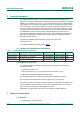


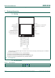
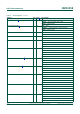
Table Of Contents
- 1. General description
- 2. Features and benefits
- 3. Applications
- 4. Overview
- 5. Marking
- 6. Block diagram
- 7. Pinning information
- 8. Functional description
- 9. Limiting values
- 10. Recommended operating conditions
- 11. Characteristics
- 12. Federal Communication Commission Statement
- 13. Industry Canada statement
- 14. Footprint information for reflow soldering
- 15. Package outline
- 16. Abbreviations
- 17. References
- 18. Legal information
- 19. Tables
- 20. Figures
- 21. Contents

UM11016 All information provided in this document is subject to legal disclaimers. © NXP Semiconductors N.V. 2016. All rights reserved.
User manual Rev. 1.0 — 15 June 2016 6 of 24
NXP Semiconductors
UM11016
ZigBee PRO and IEEE802.15.4 JN5169-001-M0x-2 modules
develop and manufacture wireless control or sensing products is to connect a power
supply and peripherals such as switches, actuators and sensors, considerably simplifying
product development.
3 module variants are available:
• JN5169-001-M00-2 with an integrated printed antenna
• JN5169-001-M03-2 with a FL antenna connector
• JN5169-001-M06-2 with a FL antenna connector and also a power amplifier and
LNA for extended range
5. Marking
5.1 JN5169-001-M00-2 and JN5169-001-M03-2
[1] With x = 0 or 3.
The JN5169-001-M0x-2 (with x = 0 or 3) family modules meet the requirements of
Directive 2002/95/EC of the European Parliament and of the Council on the Restriction of
Hazardous Substance (RoHS) and of the Chinese RoHS requirements SJ/T11363-2006
which came into force on 1st March 2007.
Fig 1. JN5169-001-M00-2 and JN5169-001-M03-2 packages marking (top view)
Table 2. Marking code
Line number Marking code
Line 1 NXP Logo: B&W outline logo
Line 2 part ID: JN5169-001-M0x-2
[1]
Line 3 serial number: NNNNN
Line 4 PMC code: ZbHYWW
Z: SSMC
b: SPIL
H: Halogen free
Y: year
WW: week
Line 5 FCC ID: XXMJN5169MxV2
[1]
Line 6 IC: 8764A-JN5169Mx
[1]
JN5169-001-M0x-2
(1)
FCC ID:XXMJN5169MxV2
(1)
NNNNN
ZbHYWW
IC: 8764A-JN5169Mx
(1)