
Datasheet


LPC111X All information provided in this document is subject to legal disclaimers. © NXP Semiconductors N.V. 2014. All rights reserved.
Product data sheet Rev. 9.2 — 26 March 2014 32 of 127
NXP Semiconductors
LPC1110/11/12/13/14/15
32-bit ARM Cortex-M0 microcontroller
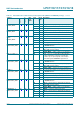
[1] Pin state at reset for default function: I = Input; O = Output; PU = internal pull-up enabled (pins pulled up to 2.6 V for
LPC111x/101/201/301, pins pulled up to full V
DD
level on LPC111x/002/102/202/302 (V
DD
= 3.3 V)); IA = inactive, no pull-up/down
enabled.
[2] 5 V tolerant pad. RESET
functionality is not available in Deep power-down mode. Use the WAKEUP pin to reset the chip and wake up
from Deep power-down mode. An external pull-up resistor is required on this pin for the Deep power-down mode. See Figure 52
for the
reset pad configuration.
[3] 5 V tolerant pad providing digital I/O functions with configurable pull-up/pull-down resistors and configurable hysteresis (see Figure 51
).
[4] I
2
C-bus pads compliant with the I
2
C-bus specification for I
2
C standard mode and I
2
C Fast-mode Plus. The pin requires an external
pull-up to provide output functionality. When power is switched off, this pin is floating and does not disturb the I2C lines. Open-drain
configuration applies to all functions on this pin.
[5] 5 V tolerant pad providing digital I/O functions with configurable pull-up/pull-down resistors, configurable hysteresis, and analog input.
When configured as a ADC input, digital section of the pad is disabled and the pin is not 5 V tolerant (see Figure 51
).
[6] When the system oscillator is not used, connect XTALIN and XTALOUT as follows: XTALIN can be left floating or can be grounded
(grounding is preferred to reduce susceptibility to noise). XTALOUT should be left floating.
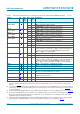
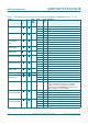
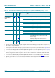
PIO3_0 to PIO3_5 I/O Port 3 — Port 3 is a 12-bit I/O port with individual direction and
function controls for each bit. The operation of port 3 pins
depends on the function selected through the IOCONFIG
register block. Pins PIO3_6 to PIO3_11 are not available.
PIO3_0/DTR
36
[3]
no I/O I; PU PIO3_0 — General purpose digital input/output pin.
O-DTR
— Data Terminal Ready output for UART.
PIO3_1/DSR
37
[3]
no I/O I; PU PIO3_1 — General purpose digital input/output pin.
I-DSR
— Data Set Ready input for UART.
PIO3_2/DCD
43
[3]
no I/O I; PU PIO3_2 — General purpose digital input/output pin.
I-DCD
— Data Carrier Detect input for UART.
PIO3_3/RI
48
[3]
no I/O I; PU PIO3_3 — General purpose digital input/output pin.
I-RI
— Ring Indicator input for UART.
PIO3_4 18
[3]
no I/O I; PU PIO3_4 — General purpose digital input/output pin.
PIO3_5 21
[3]
no I/O I; PU PIO3_5 — General purpose digital input/output pin.
V
DD
8; 44 - I - 3.3 V supply voltage to the internal regulator, the external rail,
and the ADC. Also used as the ADC reference voltage.
XTALIN 6
[6]
- I - Input to the oscillator circuit and internal clock generator circuits.
Input voltage must not exceed 1.8 V.
XTALOUT 7
[6]
- O - Output from the oscillator amplifier.
V
SS
5; 41 - I - Ground.
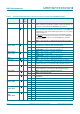
Table 8. LPC1100 and LPC1100L series: LPC1113/14 pin description table (LQFP48 package)
…continued
Symbol Pin Start
logic
input
Type Reset
state
[1]
Description