UM10398 LPC111x/LPC11Cxx User manual Rev. 12.
UM10398 NXP Semiconductors LPC111x/LPC11Cxx User manual Revision history Rev Date Description 12.3 20140610 LPC111x/LPC11C1x/LPC11C2x User manual Modifications: Section 5.2 added to describe the requirement to disable all interrupts before calling the power profiles and the requirement to use default mode when calling the IAP functions. 12.2 Modifications: 12.
UM10398 NXP Semiconductors LPC111x/LPC11Cxx User manual Revision history …continued Rev Modifications: Date Description • • • • • • LPC11D14/PCF8576D block diagram updated (see Figure 5). • • • Figure 14 updated with pseudo open-drain mode. • SRAM use by bootloader specified in Section 26.3.1. Description of interrupt use with IAP calls updated (see Section 26.4.7). SYSRSTSTAT register access changed to R/W (Table 7).
UM10398 Chapter 1: LPC111x/LPC11Cxx Introductory information Rev. 12.3 — 10 June 2014 User manual 1.1 Introduction The LPC111x/LPC11Cxx are a ARM Cortex-M0 based, low-cost 32-bit MCU family, designed for 8/16-bit microcontroller applications, offering performance, low power, simple instruction set and memory addressing together with reduced code size compared to existing 8/16-bit architectures. The LPC111x/LPC11Cxx operate at CPU frequencies of up to 50 MHz.
UM10398 NXP Semiconductors Chapter 1: LPC111x/LPC11Cxx Introductory information Table 1. LPC111x/LPC11Cxx feature changes Series Features overview • • • • • LPC1100 series LPC1100L series I2C, SSP, UART, GPIO Timers and watch dog timer 10-bit ADC Flash/SRAM memory For a full feature list, see Section 1.2. LPC1100 series features plus the following additional features: • Power profiles with lower power consumption in Active and Sleep modes.
UM10398 NXP Semiconductors Chapter 1: LPC111x/LPC11Cxx Introductory information 1.2 Features • System: – ARM Cortex-M0 processor, running at frequencies of up to 50 MHz. – ARM Cortex-M0 built-in Nested Vectored Interrupt Controller (NVIC). – Serial Wire Debug. – System tick timer. • Memory: – On-chip flash programming memory for LPC1100, LPC1100L, and LPC1100C series: 32 kB (LPC1114/LPC11C14), 24 kB (LPC1113), 16 kB (LPC1112/LPC11C12), or 8 kB (LPC1111), 4kB (LPC1110).
UM10398 NXP Semiconductors Chapter 1: LPC111x/LPC11Cxx Introductory information – Programmable watchdog oscillator with a frequency range of 7.8 kHz to 1.8 MHz. – PLL allows CPU operation up to the maximum CPU rate without the need for a high-frequency crystal. May be run from the system oscillator or the internal RC oscillator. – Clock output function with divider that can reflect the system oscillator clock, IRC clock, CPU clock, and the Watchdog clock.
UM10398 NXP Semiconductors Chapter 1: LPC111x/LPC11Cxx Introductory information 1.3 Ordering information Table 2. Ordering information Type number Package Name Description Version SO20, TSSOP20, TSSOP28, and DIP28 packages LPC1110FD20 SO20 SO20: plastic small outline package; 20 leads; body width 7.5 mm SOT163-1 LPC1111FDH20/002 TSSOP20 TSSOP20: plastic thin shrink small outline package; 20 leads; body width 4.
UM10398 NXP Semiconductors Chapter 1: LPC111x/LPC11Cxx Introductory information Table 2. Ordering information …continued Type number Package Name Description Version LPC1112FHI33/203 HVQFN33 HVQFN: plastic thermal enhanced very thin quad flat package; no leads; 33 terminals; body 5 5 0.85 mm n/a LPC1112JHI33/203 HVQFN33 HVQFN: plastic thermal enhanced very thin quad flat package; no leads; 33 terminals; body 5 5 0.
UM10398 NXP Semiconductors Chapter 1: LPC111x/LPC11Cxx Introductory information Table 2. Ordering information …continued Type number Package Name Description Version LPC1114FHN33/303 HVQFN33 HVQFN: plastic thermal enhanced very thin quad flat package; no leads; 33 terminals; body 7 7 0.85 mm n/a LPC1114JHN33/303 HVQFN33 HVQFN: plastic thermal enhanced very thin quad flat package; no leads; 33 terminals; body 7 7 0.
UM10398 NXP Semiconductors Chapter 1: LPC111x/LPC11Cxx Introductory information Series Flash UART RS-485 SPI Power profiles ADC channels GPIO C_CAN Operating temperature[1] Package I2C/ Fm+ Ordering options Total SRAM Table 3.
UM10398 NXP Semiconductors Chapter 1: LPC111x/LPC11Cxx Introductory information Series UART RS-485 SPI Power profiles ADC channels GPIO C_CAN Operating temperature[1] Package I2C/ Fm+ Ordering options …continued Type number Total SRAM Table 3.
UM10398 NXP Semiconductors Chapter 1: LPC111x/LPC11Cxx Introductory information ADC channels C_CAN Operating temperature[1] Package GPIO Flash LPC11C22FBD48/301 LPC11C00 16 kB 8 kB 1 1 2 no 8 36 1 F LQFP48 LPC11C24FBD48/301 LPC11C00 32 kB 8 kB 1 1 2 no 8 36 1 F LQFP48 1 2 yes 8 42 - F LQFP100 I2C/ Fm+ Series UART RS-485 Type number Total SRAM Power profiles Ordering options …continued SPI Table 3.
UM10398 NXP Semiconductors Chapter 1: LPC111x/LPC11Cxx Introductory information 1.
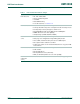
UM10398 NXP Semiconductors Chapter 1: LPC111x/LPC11Cxx Introductory information XTALIN XTALOUT RESET SWD LPC1111/12/13/14/15XL IRC TEST/DEBUG INTERFACE CLOCK GENERATION, POWER CONTROL, SYSTEM FUNCTIONS POR ARM CORTEX-M0 system bus clocks and controls FLASH 8/16/24/32/ 48/56/64 kB slave GPIO ports PIO0/1/2/3 HIGH-SPEED GPIO CLKOUT SRAM 2/4/8 kB slave ROM slave slave AHB-LITE BUS slave AHB TO APB BRIDGE RXD TXD DTR, DSR(1), CTS, (1) (1) DCD , RI , RTS CT32B0_MAT[3:0] CT32B0_CAP[1:0] CT32B1_MA
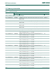
UM10398 NXP Semiconductors Chapter 1: LPC111x/LPC11Cxx Introductory information XTALIN XTALOUT RESET SWD LPC11Cxx LPC11D14 IRC TEST/DEBUG INTERFACE CLOCK GENERATION, POWER CONTROL, SYSTEM FUNCTIONS POR ARM CORTEX-M0 system bus clocks and controls FLASH 16/32 kB slave HIGH-SPEED GPIO GPIO ports PIO0/1/2/3 CLKOUT SRAM 8 kB slave ROM slave slave AHB-LITE BUS slave AHB TO APB BRIDGE RXD TXD DTR, DSR, CTS, DCD, RI, RTS CT32B0_MAT[3:0] CT32B0_CAP0 CT32B1_MAT[3:0] CT32B1_CAP0 CT16B0_MAT[2:0] CT16
UM10398 NXP Semiconductors Chapter 1: LPC111x/LPC11Cxx Introductory information S[39:0] PIO0, PIO1, PIO2, PIO3 BP[3:0] PCF8576D LPC1114 LCD CONTROLLER MCU VLCD Fig 4.
UM10398 NXP Semiconductors Chapter 1: LPC111x/LPC11Cxx Introductory information 1.5 ARM Cortex-M0 processor The ARM Cortex-M0 processor is described in detail in Section 28.3 “About the Cortex-M0 processor and core peripherals”. For the LPC111x/LPC11Cxx, the ARM Cortex-M0 processor core is configured as follows: • System options: – The Nested Vectored Interrupt Controller (NVIC) is included and supports up to 32 interrupts. – The system tick timer is included.
UM10398 Chapter 2: LPC111x/LPC11Cxx Memory mapping Rev. 12.3 — 10 June 2014 User manual 2.1 How to read this chapter Table 4 and Table 5 show the memory configurations for different LPC111x/LPC11Cxx parts. Table 4.
UM10398 NXP Semiconductors Chapter 2: LPC111x/LPC11Cxx Memory mapping LPC1111/12/13/14 LPC11Cxx LPC11D14 4 GB AHB peripherals 0x5020 0000 0xFFFF FFFF reserved 16 - 127 reserved 0xE010 0000 private peripheral bus 0x5004 0000 0xE000 0000 12-15 GPIO PIO3 0x5020 0000 8-11 GPIO PIO2 0x5000 0000 4-7 GPIO PIO1 0-3 GPIO PIO0 reserved AHB peripherals APB peripherals reserved 0x5003 0000 0x5002 0000 0x5001 0000 0x5000 0000 0x4008 0000 23 - 31 reserved 0x4005 C000 0x4008 0000 APB peripherals 1
UM10398 NXP Semiconductors Chapter 2: LPC111x/LPC11Cxx Memory mapping 4 GB AHB peripherals LPC1111/12/13/14/15XL 0x5020 0000 0xFFFF FFFF reserved 0xE010 0000 private peripheral bus 127-16 reserved 0xE000 0000 0x5004 0000 reserved 0x5020 0000 AHB peripherals 0x5000 0000 12-15 GPIO PIO3 8-11 GPIO PIO2 4-7 GPIO PIO1 0-3 GPIO PIO0 reserved APB peripherals 0x5003 0000 0x5002 0000 0x5001 0000 0x5000 0000 0x4008 0000 31-23 reserved 0x4005 C000 0x4008 0000 1 GB APB peripherals SPI1 22 0
UM10398 Chapter 3: LPC111x/LPC11Cxx System configuration (SYSCON) Rev. 12.3 — 10 June 2014 User manual 3.1 How to read this chapter The following functions of the system configuration block depend on the specific part number: DEVICE_ID register The DEVICE_ID register is valid 0x4004 83F4 for parts of the LPC1100, LPC1100C, and LPC1100L series only. The device ID cannot be read through the SYSCON block for the LPC1100XL series.
UM10398 NXP Semiconductors Chapter 3: LPC111x/LPC11Cxx System configuration (SYSCON) Table 6. Pin summary Pin name Pin direction Pin description CLKOUT O Clockout pin PIO0_0 to PIO0_11 I Start logic wake-up pins port 0 PIO1_0 I Start logic wake-up pin port 1 3.4 Clock generation See Figure 8 for an overview of the LPC111x/LPC11Cxx Clock Generation Unit (CGU). The LPC111x/LPC11Cxx include three independent oscillators.
UM10398 NXP Semiconductors Chapter 3: LPC111x/LPC11Cxx System configuration (SYSCON) ARM CORTEX-M0 SYSTEM CLOCK DIVIDER system clock 18 SYSAHBCLKDIV SYSAHBCLKCTRL[1:18] IRC oscillator AHB clocks 1 to 18 (memories and peripherals) SPI0 PERIPHERAL CLOCK DIVIDER SPI0_PCLK UART PERIPHERAL CLOCK DIVIDER UART_PCLK SPI1 PERIPHERAL CLOCK DIVIDER SPI1_PCLK main clock watchdog oscillator MAINCLKSEL (main clock select) sys_pllclkout IRC oscillator IRC oscillator sys_pllclkin system oscillator SYST
UM10398 NXP Semiconductors Chapter 3: LPC111x/LPC11Cxx System configuration (SYSCON) Table 7.
UM10398 NXP Semiconductors Chapter 3: LPC111x/LPC11Cxx System configuration (SYSCON) Table 7.
UM10398 NXP Semiconductors Chapter 3: LPC111x/LPC11Cxx System configuration (SYSCON) Table 9. Peripheral reset control register (PRESETCTRL, address 0x4004 8004) bit description Bit Symbol 0 SSP0_RST_N 1 2 3 31:4 Value Description Reset value SPI0 reset control 0 0 Resets the SPI0 peripheral. 1 SPI0 reset de-asserted. I2C_RST_N I2C reset control 0 Resets the I2C peripheral. 1 I2C reset de-asserted. 0 Resets the SPI1 peripheral. 1 SPI1 reset de-asserted.
UM10398 NXP Semiconductors Chapter 3: LPC111x/LPC11Cxx System configuration (SYSCON) Table 11. System PLL status register (SYSPLLSTAT, address 0x4004 800C) bit description Bit Symbol 0 LOCK 31:1 Value - Description Reset value PLL lock status 0x0 0 PLL not locked 1 PLL locked - Reserved 0x00 3.5.5 System oscillator control register This register configures the frequency range for the system oscillator. Table 12.
UM10398 NXP Semiconductors Chapter 3: LPC111x/LPC11Cxx System configuration (SYSCON) Table 13. Watchdog oscillator control register (WDTOSCCTRL, address 0x4004 8024) bit description Bit Symbol 4:0 8:5 31:9 Description Reset value DIVSEL Select divider for Fclkana. wdt_osc_clk = Fclkana/ (2 (1 + DIVSEL)) 00000: 2 (1 + DIVSEL) = 2 00001: 2 (1 + DIVSEL) = 4 to 11111: 2 (1 + DIVSEL) = 64 0 FREQSEL Select watchdog oscillator analog output frequency (Fclkana). 0x00 - Value 0x1 0.
UM10398 NXP Semiconductors Chapter 3: LPC111x/LPC11Cxx System configuration (SYSCON) The reset value given in Table 15 applies to the POR reset. Table 15. System reset status register (SYSRSTSTAT, address 0x4004 8030) bit description Bit Symbol 0 POR 1 2 3 4 31:5 Value Description Reset value POR reset status 0x0 0 No POR detected. 1 POR detected. Writing a one clears this reset. Status of the external RESET pin. EXTRST 0x0 0 No RESET event detected. 1 RESET detected.
UM10398 NXP Semiconductors Chapter 3: LPC111x/LPC11Cxx System configuration (SYSCON) 3.5.10 System PLL clock source update enable register This register updates the clock source of the system PLL with the new input clock after the SYSPLLCLKSEL register has been written to. In order for the update to take effect, first write a zero to the SYSPLLUEN register and then write a one to SYSPLLUEN. Remark: When switching clock sources, both clocks must be running before the clock source is updated. Table 17.
UM10398 NXP Semiconductors Chapter 3: LPC111x/LPC11Cxx System configuration (SYSCON) Table 19. Main clock source update enable register (MAINCLKUEN, address 0x4004 8074) bit description Bit Symbol 0 ENA 31:1 Value - Description Reset value Enable main clock source update 0x0 0 No change 1 Update clock source - Reserved 0x00 3.5.13 System AHB clock divider register This register divides the main clock to provide the system clock to the core, memories, and the peripherals.
UM10398 NXP Semiconductors Chapter 3: LPC111x/LPC11Cxx System configuration (SYSCON) Table 21. System AHB clock control register (SYSAHBCLKCTRL, address 0x4004 8080) bit description …continued Bit Symbol 4 FLASHARRAY 5 6 7 8 9 10 Value Description Reset value Enables clock for flash array access. 1 0 Disabled 1 Enabled I2C Enables clock for I2C. 0 Disable 1 Enable GPIO Enables clock for GPIO.
UM10398 NXP Semiconductors Chapter 3: LPC111x/LPC11Cxx System configuration (SYSCON) Table 21. System AHB clock control register (SYSAHBCLKCTRL, address 0x4004 8080) bit description …continued Bit Symbol 17 CAN 18 31:19 Value Reset value Enables clock for C_CAN. See Section 3.1 for part specific details. 0 0 Disable 1 Enable SSP1 - Description Enables clock for SPI1. 0 Disable 1 Enable - Reserved 0 0x00 3.5.
UM10398 NXP Semiconductors Chapter 3: LPC111x/LPC11Cxx System configuration (SYSCON) Table 24. SPI1 clock divider register (SSP1CLKDIV, address 0x4004 809C) bit description Bit Symbol Description Reset value 7:0 DIV SPI1_PCLK clock divider values 0: Disable SPI1_PCLK. 1: Divide by 1. to 255: Divide by 255. 0x00 31:8 - Reserved 0x00 3.5.18 WDT clock source select register This register selects the clock source for the watchdog timer. The WDTCLKUEN register (see Section 3.5.
UM10398 NXP Semiconductors Chapter 3: LPC111x/LPC11Cxx System configuration (SYSCON) Table 27. WDT clock divider register (WDTCLKDIV, address 0x4004 80D8) bit description Bit Symbol Description Reset value 7:0 DIV WDT clock divider values 0: Disable WDCLK. 1: Divide by 1. to 255: Divide by 255. 0x00 31:8 - Reserved 0x00 3.5.21 CLKOUT clock source select register This register configures the clkout_clk signal to be output on the CLKOUT pin.
UM10398 NXP Semiconductors Chapter 3: LPC111x/LPC11Cxx System configuration (SYSCON) 3.5.23 CLKOUT clock divider register This register determines the divider value for the clock output signal on the CLKOUT pin. Table 30. CLKOUT clock divider registers (CLKOUTCLKDIV, address 0x4004 80E8) bit description Bit Symbol Description Reset value 7:0 DIV Clock output divider values 0: Disable CLKOUT. 1: Divide by 1. to 255: Divide by 255. 0x00 31:8 - Reserved 0x00 3.5.
UM10398 NXP Semiconductors Chapter 3: LPC111x/LPC11Cxx System configuration (SYSCON) 3.5.26 BOD control register The BOD control register selects up to four separate threshold values for sending a BOD interrupt to the NVIC and for forced reset. Reset and interrupt threshold values listed are typical values. Table 33.
UM10398 NXP Semiconductors Chapter 3: LPC111x/LPC11Cxx System configuration (SYSCON) Setting this parameter to a very low value (e.g. zero) will guarantee the best possible interrupt performance but will also introduce a significant degree of uncertainty and jitter. Requiring the system to always take a larger number of cycles (whether it needs it or not) will reduce the amount of uncertainty but may not necessarily eliminate it.
UM10398 NXP Semiconductors Chapter 3: LPC111x/LPC11Cxx System configuration (SYSCON) Remark: Each interrupt connected to a start logic input must be enabled in the NVIC if the corresponding PIO pin is used to wake up the chip from Deep-sleep mode. Table 37.
UM10398 NXP Semiconductors Chapter 3: LPC111x/LPC11Cxx System configuration (SYSCON) 3.5.33 Start logic status register 0 This register reflects the status of the enabled start signal bits. The bit assignment is identical to Table 37. Each bit (if enabled) reflects the state of the start logic, i.e. whether or not a wake-up signal has been received for a given pin. Table 40.
UM10398 NXP Semiconductors Chapter 3: LPC111x/LPC11Cxx System configuration (SYSCON) Table 42. Deep-sleep configuration register (PDSLEEPCFG, address 0x4004 8230) bit description Bit Symbol 2:0 3 Value Description Reset value NOTUSED Reserved. Always write these bits as 111. 0 BOD_PD BOD power-down control in Deep-sleep mode, see Table 41. 0 0 Powered 1 Powered down 5:4 NOTUSED Reserved. Always write these bits as 11.
UM10398 NXP Semiconductors Chapter 3: LPC111x/LPC11Cxx System configuration (SYSCON) Table 43.
UM10398 NXP Semiconductors Chapter 3: LPC111x/LPC11Cxx System configuration (SYSCON) Table 44.
UM10398 NXP Semiconductors Chapter 3: LPC111x/LPC11Cxx System configuration (SYSCON) – 0x1A07 102B = LPC1110FD20 • LPC1111 – 0x0A16 D02B = LPC1111FDH20/002 – 0x1A16 D02B = LPC1111FDH20/002 – 0x041E 502B = LPC1111FHN33/101 – 0x2516 D02B = LPC1111FHN33/101; LPC1111FHN33/102 – 0x0416 502B = LPC1111FHN33/201 – 0x2516 902B = LPC1111FHN33/201; LPC1111FHN33/202 • LPC1112 – 0x0A24 902B = LPC1112FD20/102; LPC1112FDH20/102; LPC1112FDH28/102 – 0x1A24 902B = LPC1112FD20/102; LPC1112FDH20/102; LPC1112FDH28/102 – 0x
UM10398 NXP Semiconductors Chapter 3: LPC111x/LPC11Cxx System configuration (SYSCON) 3.6 Reset Reset has four sources on the LPC111x/LPC11Cxx: the RESET pin, Watchdog Reset, Power-On Reset (POR), and Brown Out Detect (BOD). In addition, there is an ARM software reset. The RESET pin is a Schmitt trigger input pin.
UM10398 NXP Semiconductors Chapter 3: LPC111x/LPC11Cxx System configuration (SYSCON) IRC starts IRC status internal reset VDD valid threshold = 1.8V 80 μs 101 μs GND boot time supply ramp-up time 55 μs user code processor status boot code execution finishes; user code starts Fig 9. Start-up timing 3.8 Brown-out detection The LPC111x/LPC11Cxx includes up to four levels for monitoring the voltage on the VDD pin.
UM10398 NXP Semiconductors Chapter 3: LPC111x/LPC11Cxx System configuration (SYSCON) The chip is in Active mode after reset and the default power configuration is determined by the reset values of the PDRUNCFG and SYSAHBCLKCTRL registers. The power configuration can be changed during run time. 3.9.1.
UM10398 NXP Semiconductors Chapter 3: LPC111x/LPC11Cxx System configuration (SYSCON) 3.9.2.3 Wake-up from Sleep mode Sleep mode is exited automatically when an interrupt enabled by the NVIC arrives at the processor or a reset occurs. After wake-up due to an interrupt, the microcontroller returns to its original power configuration defined by the contents of the PDRUNCFG and the SYSAHBCLKDIV registers. If a reset occurs, the microcontroller enters the default configuration in Active mode. 3.9.
UM10398 NXP Semiconductors Chapter 3: LPC111x/LPC11Cxx System configuration (SYSCON) 4. If an external pin is used for wake-up, enable and clear the wake-up pin in the start logic registers (Table 37 to Table 40), and enable the start logic interrupt in the NVIC. 5. In the SYSAHBCLKCTRL register (Table 21), disable all peripherals except counter/timer or WDT if needed. 6. Write one to the SLEEPDEEP bit in the ARM Cortex-M0 SCR register (Table 453). 7. Use the ARM WFI instruction. 3.9.3.
UM10398 NXP Semiconductors Chapter 3: LPC111x/LPC11Cxx System configuration (SYSCON) 1. Write one to the DPDEN bit in the PCON register (see Table 50). 2. Store data to be retained in the general purpose registers (Table 51). 3. Write one to the SLEEPDEEP bit in the ARM Cortex-M0 SCR register (Table 453). 4. Ensure that the IRC is powered by setting bits IRCOUT_PD and IRC_PD to zero in the PDRUNCFG register before entering Deep power-down mode. Remark: This step is part dependent. See Section 3.
UM10398 NXP Semiconductors Chapter 3: LPC111x/LPC11Cxx System configuration (SYSCON) set the appropriate edge polarity for the corresponding wake-up event. Furthermore, the interrupts corresponding to each input must be enabled in the NVIC. Interrupts 0 to 12 in the NVIC correspond to 13 PIO pins (see Section 3.5.30). The start logic does not require a clock to run because it uses the input signals on the enabled pins to generate a clock edge when enabled.
UM10398 NXP Semiconductors Chapter 3: LPC111x/LPC11Cxx System configuration (SYSCON) irc_osc_clk FCLKIN sys_osc_clk pd FCCO PSEL<1:0> PFD 2 SYSPLLCLKSEL pd LOCK DETECT LOCK cd /2P FCLKOUT analog section pd cd /M 5 MSEL<4:0> Fig 10. System PLL block diagram The block diagram of this PLL is shown in Figure 10. The input frequency range is 10 MHz to 25 MHz. The input clock is fed directly to the Phase-Frequency Detector (PFD).
UM10398 NXP Semiconductors Chapter 3: LPC111x/LPC11Cxx System configuration (SYSCON) stopped and the dividers will enter a reset state. While in Power-down mode, the lock output will be low to indicate that the PLL is not in lock. When the Power-down mode is terminated by setting the SYSPLL_PD bits to zero, the PLL will resume its normal operation and will make the lock signal high once it has regained lock on the input clock. 3.11.
UM10398 NXP Semiconductors Chapter 3: LPC111x/LPC11Cxx System configuration (SYSCON) 1. Specify the input clock frequency FCLKIN. 2. Calculate M to obtain the desired output frequency FCLKOUT with M = FCLKOUT / FCLKIN. 3. Find a value so that FCCO = 2 P FCLKOUT. 4. Verify that all frequencies and divider values conform to the limits specified in Table 10. 5. Ensure that FCLKOUT < 100 MHz. Table 47 shows how to configure the PLL for a 12 MHz crystal oscillator using the SYSPLLCTRL register (Table 10).
UM10398 NXP Semiconductors Chapter 3: LPC111x/LPC11Cxx System configuration (SYSCON) Table 48. Bit Symbol 1:0 FLASHTIM 31:2 - UM10398 User manual Flash configuration register (FLASHCFG, address 0x4003 C010) bit description Value Description Reset value Flash memory access time. FLASHTIM +1 is equal to the number of system clocks used for flash access. 10 00 1 system clock flash access time (for system clock frequencies of up to 20 MHz).
UM10398 Chapter 4: LPC111x/LPC11Cxx Power Monitor Unit (PMU) Rev. 12.3 — 10 June 2014 User manual 4.1 How to read this chapter Remark: For parts LPC11(D)1x/102/202/302, also refer to Chapter 5 for power control. 4.2 Introduction The PMU controls the Deep power-down mode. Four general purpose register in the PMU can be used to retain data during Deep power-down mode. 4.3 Register description Table 49.
UM10398 NXP Semiconductors Chapter 4: LPC111x/LPC11Cxx Power Monitor Unit (PMU) Table 50. Power control register (PCON, address 0x4003 8000) bit description …continued Bit Symbol Value 8 SLEEPFLAG 10:9 - 11 DPDFLAG 31:12 - Description Reset value Sleep mode flag 0 0 Read: No power-down mode entered. LPC111x/LPC11Cxx is in Active mode. Write: No effect. 1 Read: Sleep/Deep-sleep or Deep power-down mode entered. Write: Writing a 1 clears the SLEEPFLAG bit to 0. - Reserved.
UM10398 NXP Semiconductors Chapter 4: LPC111x/LPC11Cxx Power Monitor Unit (PMU) Table 52. General purpose register 4 (GPREG4, address 0x4003 8014) bit description Bit Symbol 10 WAKEUPHYS 31:11 Value GPDATA Description Reset value WAKEUP pin hysteresis enable 0x0 1 Hysteresis for WAKEUP pin enabled. 0 Hysteresis for WAKUP pin disabled. Data retained during Deep power-down mode. 0x0 4.4 Functional description For details of entering and exiting Deep power-down mode, see Section 3.9.4.
UM10398 Chapter 5: LPC111x/LPC11Cxx Power profiles Rev. 12.3 — 10 June 2014 User manual 5.1 How to read this chapter The power profiles are available for parts LPC11(D)1x/102/202/302 only (LPC1100L series). 5.2 Basic configuration Specific power profile settings are required in the following situation: When using IAP commands, configure the power profiles in Default mode. Disable all interrupts before making calls to the power profile API.
UM10398 NXP Semiconductors Chapter 5: LPC111x/LPC11Cxx Power profiles Power API function table set_pll Ptr to ROM Driver table 0x1FFF 2004 set_power ROM Driver Table 0x1FFF 1FF8 Ptr to Device Table 0 0x1FFF 1FFC Ptr to Device Table 1 0x1FFF 2000 Ptr to Device Table 2 Device n 0x1FFF 2004 Ptr to Function 0 Ptr to PowerAPI Table Ptr to Function 1 Ptr to Function 2 … … Ptr to Function n Ptr to Device Table n Fig 11.
UM10398 NXP Semiconductors Chapter 5: LPC111x/LPC11Cxx Power profiles typedef struct _PWRD { void (*set_pll)(unsigned int cmd[], unsigned int resp[]); void (*set_power)(unsigned int cmd[], unsigned int resp[]); } PWRD; typedef struct _ROM { const PWRD * pWRD; } ROM; ROM ** rom = (ROM **) (0x1FFF1FF8 + 3 * sizeof(ROM**)); unsigned int command[4], result[2]; 5.6 Clocking routine 5.6.1 set_pll This routine sets up the system PLL according to the calling arguments.
UM10398 NXP Semiconductors Chapter 5: LPC111x/LPC11Cxx Power profiles /* set_pll result0 options */ #define PLL_CMD_SUCCESS #define PLL_INVALID_FREQ #define PLL_INVALID_MODE #define PLL_FREQ_NOT_FOUND #define PLL_NOT_LOCKED 0 1 2 3 4 For a simplified clock configuration scheme see Figure 12. For more details see Figure 8. 5.6.1.1 Param0: system PLL input frequency and Param1: expected system clock set_pll looks for a setup in which the system PLL clock does not exceed 50 MHz.
UM10398 NXP Semiconductors Chapter 5: LPC111x/LPC11Cxx Power profiles supply and/or ambient temperature. This is why it is suggested that when a good known clock source is used and a PLL_NOT_LOCKED response is received, the set_pll routine should be invoked several times before declaring the selected PLL clock source invalid. Hint: setting Param3 equal to the system PLL frequency [Hz] divided by 10000 will provide more than enough PLL lock-polling cycles. 5.6.1.
UM10398 NXP Semiconductors Chapter 5: LPC111x/LPC11Cxx Power profiles 5.6.1.4.4 System clock less than or equal to the expected value command[0] = 12000; command[1] = 25000; command[2] = CPU_FREQ_LTE; command[3] = 0; (*rom)->pWRD->set_pll(command, result); The above code specifies a 12 MHz PLL input clock, a system clock of no more than 25 MHz and no locking time-out. set_pll returns PLL_CMD_SUCCESS in result[0] and 24000 in result[1]. The new system clock is 24 MHz. 5.6.1.4.
UM10398 NXP Semiconductors Chapter 5: LPC111x/LPC11Cxx Power profiles using power profiles and changing system clock current_clock, new_clock , new_mode use power routine call to change mode to DEFAULT use either clocking routine call or custom code to change system clock from current_clock to new_clock use power routine call to change mode to new_mode end Fig 13. Power profiles usage Table 54.
UM10398 NXP Semiconductors Chapter 5: LPC111x/LPC11Cxx Power profiles For a simplified clock configuration scheme see Figure 12. For more details see Figure 8. 5.7.1.1 Param0: main clock The main clock is the clock rate the microcontroller uses to source the system’s and the peripherals’ clock. It is configured by either a successful execution of the clocking routine call or a similar code provided by the user. This operand must be an integer between 1 to 50 MHz inclusive.
UM10398 NXP Semiconductors Chapter 5: LPC111x/LPC11Cxx Power profiles (*rom)->pWRD->set_power(command, result); The above code specifies that an application is running at the main and system clock of 24 MHz with emphasis on efficiency. set_power returns PWR_CMD_SUCCESS in result[0] after configuring the microcontroller’s internal power control features. UM10398 User manual All information provided in this document is subject to legal disclaimers. Rev. 12.3 — 10 June 2014 © NXP B.V. 2014.
UM10398 Chapter 6: LPC111x/LPC11Cxx Nested Vectored Interrupt Controller (NVIC) Rev. 12.3 — 10 June 2014 User manual 6.1 How to read this chapter The C_CAN controller interrupt is available on parts LPC11Cxx only. 6.2 Introduction The Nested Vectored Interrupt Controller (NVIC) is an integral part of the Cortex-M0. The tight coupling to the CPU allows for low interrupt latency and efficient processing of late arriving interrupts. 6.
UM10398 NXP Semiconductors Chapter 6: LPC111x/LPC11Cxx Nested Vectored Interrupt Controller Table 55.
UM10398 Chapter 7: LPC1100/LPC1100C/LPC1100L series: I/O configuration (IOCONFIG) Rev. 12.3 — 10 June 2014 User manual 7.1 How to read this chapter Remark: This chapter applies to parts in the following series (see Table 1): • • • • LPC1100 LPC1100L LPC1100C LPC11D14 Pin configuration The implementation of the I/O configuration registers varies for different LPC111x/LPC11Cxx parts and packages. Table 57 shows which IOCON registers are used on the different packages.
UM10398 NXP Semiconductors Chapter 7: LPC1100/LPC1100C/LPC1100L series: I/O configuration • Pseudo open-drain mode for non-I2C pins (see Section 7.1 for part specific details). 7.3 General description The IOCON registers control the function (GPIO or peripheral function), the input mode, and the hysteresis of all PIOn_m pins. In addition, the I2C-bus pins can be configured for different I2C-bus modes. If a pin is used as input pin for the ADC, an analog input mode can be selected.
UM10398 NXP Semiconductors Chapter 7: LPC1100/LPC1100C/LPC1100L series: I/O configuration 7.3.2 Pin mode The MODE bits in the IOCON register allow the selection of on-chip pull-up or pull-down resistors for each pin or select the repeater mode. The possible on-chip resistor configurations are pull-up enabled, pull-down enabled, or no pull-up/pull-down. The default value is pull-up enabled. See Section 7.1 for part specific details.
UM10398 NXP Semiconductors Chapter 7: LPC1100/LPC1100C/LPC1100L series: I/O configuration 7.3.6 Open-drain Mode When output is selected, either by selecting a special function in the FUNC field, or by selecting GPIO function for a pin having a 1 in its GPIODIR register, a 1 in the OD bit selects open-drain operation, that is, a 1 disables the high-drive transistor. This option has no effect on the primary I2C pins. Remark: The open-drain mode is not available on all parts (see Section 7.1). 7.
UM10398 NXP Semiconductors Chapter 7: LPC1100/LPC1100C/LPC1100L series: I/O configuration Table 56.
UM10398 NXP Semiconductors Chapter 7: LPC1100/LPC1100C/LPC1100L series: I/O configuration Table 56.
UM10398 NXP Semiconductors Chapter 7: LPC1100/LPC1100C/LPC1100L series: I/O configuration Table 57.
UM10398 NXP Semiconductors Chapter 7: LPC1100/LPC1100C/LPC1100L series: I/O configuration Table 58. IOCON_PIO2_6 register (IOCON_PIO2_6, address 0x4004 4000) bit description Bit Symbol 10 OD 31:11 - Value Description Reset value Selects pseudo open-drain mode. See Section 7.1 for part specific details. 0 0 Standard GPIO output 1 Open-drain output - Reserved - 7.4.2 IOCON_PIO2_0 Table 59.
UM10398 NXP Semiconductors Chapter 7: LPC1100/LPC1100C/LPC1100L series: I/O configuration Table 60. IOCON_RESET_PIO0_0 register (IOCON_RESET_PIO0_0, address 0x4004 400C) bit description Bit Symbol 4:3 MODE 5 Value 10 OD 31:11 - Selects function mode (on-chip pull-up/pull-down resistor control). 10 Inactive (no pull-down/pull-up resistor enabled). 0x1 Pull-down resistor enabled. 0x2 Pull-up resistor enabled. 0x3 Repeater mode. Hysteresis.
UM10398 NXP Semiconductors Chapter 7: LPC1100/LPC1100C/LPC1100L series: I/O configuration 7.4.5 IOCON_PIO1_8 Table 62. IOCON_PIO1_8 register (IOCON_PIO1_8, address 0x4004 4014) bit description Bit Symbol 2:0 FUNC 4:3 5 OD - Reset value Selects pin function. All other values are reserved. 000 Selects function PIO1_8. 0x1 Selects function CT16B1_CAP0. Selects function mode (on-chip pull-up/pull-down resistor control). 0x0 Inactive (no pull-down/pull-up resistor enabled).
UM10398 NXP Semiconductors Chapter 7: LPC1100/LPC1100C/LPC1100L series: I/O configuration Table 63. IOCON_PIO0_2 register (IOCON_PIO0_2, address 0x4004 401C) bit description Bit Symbol 10 OD 31:11 - Value Description Reset value Selects pseudo open-drain mode. See Section 7.1 for part specific details. 0 0 Standard GPIO output 1 Open-drain output - Reserved - 7.4.7 IOCON_PIO2_7 Table 64.
UM10398 NXP Semiconductors Chapter 7: LPC1100/LPC1100C/LPC1100L series: I/O configuration Table 65. IOCON_PIO2_8 register (IOCON_PIO2_8, address 0x4004 4024) bit description Bit Symbol 5 HYS 9:6 - 10 OD 31:11 - Value Description Reset value Hysteresis. 0 0 Disable. 1 Enable. - Reserved 0011 Selects pseudo open-drain mode. See Section 7.1 for part specific details. 0 0 Standard GPIO output 1 Open-drain output - Reserved - 7.4.9 IOCON_PIO2_1 Table 66.
UM10398 NXP Semiconductors Chapter 7: LPC1100/LPC1100C/LPC1100L series: I/O configuration 7.4.10 IOCON_PIO0_3 Table 67. IOCON_PIO0_3 register (IOCON_PIO0_3, address 0x4004 402C) bit description Bit Symbol 2:0 FUNC Value 0x0 4:3 5 10 OD 31:11 Selects pin function. All other values are reserved. 000 Selects function mode (on-chip pull-up/pull-down resistor control). 0x0 Inactive (no pull-down/pull-up resistor enabled). 0x1 Pull-down resistor enabled. 0x2 Pull-up resistor enabled.
UM10398 NXP Semiconductors Chapter 7: LPC1100/LPC1100C/LPC1100L series: I/O configuration 7.4.12 IOCON_PIO0_5 Table 69. IOCON_PIO0_5 register (IOCON_PIO0_5, address 0x4004 4034) bit description Bit Symbol 2:0 FUNC Value 7:3 9:8 Selects pin function. All other values are reserved. 000 Selects function PIO0_5 (open-drain pin). 0x1 Selects I2C function SDA (open-drain pin). - Reserved. 00000 Selects I2C mode.
UM10398 NXP Semiconductors Chapter 7: LPC1100/LPC1100C/LPC1100L series: I/O configuration Table 71. IOCON_PIO3_4 register (IOCON_PIO3_4, address 0x4004 403C) bit description Bit Symbol 2:0 FUNC Value 0x0 4:3 5 OD 31:11 - Selects pin function. All other values are reserved. 000 Selects function mode (on-chip pull-up/pull-down resistor control). 0x0 Inactive (no pull-down/pull-up resistor enabled). 0x1 Pull-down resistor enabled. 0x2 Pull-up resistor enabled. 0x3 Repeater mode.
UM10398 NXP Semiconductors Chapter 7: LPC1100/LPC1100C/LPC1100L series: I/O configuration 7.4.16 IOCON_PIO2_5 Remark: See Section 7.1 for part specific details. Table 73. IOCON_PIO2_5 register (IOCON_PIO2_5, address 0x4004 4044) bit description Bit Symbol 2:0 FUNC 4:3 MODE Value 0x0 5 10 OD 31:11 - Selects pin function. All other values are reserved. 000 Selects function PIO2_5. 0x0 Inactive (no pull-down/pull-up resistor enabled). 0x1 Pull-down resistor enabled.
UM10398 NXP Semiconductors Chapter 7: LPC1100/LPC1100C/LPC1100L series: I/O configuration Table 74. IOCON_PIO3_5 register (IOCON_PIO3_5, address 0x4004 4048) bit description Bit Symbol 10 OD 31:11 - Value Description Reset value Selects pseudo open-drain mode. See Section 7.1 for part specific details. 0 0 Standard GPIO output 1 Open-drain output - Reserved - 7.4.18 IOCON_PIO0_6 Table 75.
UM10398 NXP Semiconductors Chapter 7: LPC1100/LPC1100C/LPC1100L series: I/O configuration Table 76. IOCON_PIO0_7 register (IOCON_PIO0_7, address 0x4004 4050) bit description Bit Symbol 4:3 MODE 5 - 10 OD - Description Reset value Selects function mode (on-chip pull-up/pull-down resistor control). 10 0x0 Inactive (no pull-down/pull-up resistor enabled). 0x1 Pull-down resistor enabled. 0x2 Pull-up resistor enabled. 0x3 Repeater mode. HYS 9:6 31:11 Value Hysteresis.
UM10398 NXP Semiconductors Chapter 7: LPC1100/LPC1100C/LPC1100L series: I/O configuration 7.4.21 IOCON_PIO2_10 Table 78. IOCON_PIO2_10 register (IOCON_PIO2_10, address 0x4004 4058) bit description Bit Symbol 2:0 FUNC Value 0x0 4:3 5 10 OD 31:11 - Selects pin function. All other values are reserved. 000 Selects function mode (on-chip pull-up/pull-down resistor control). 0x0 Inactive (no pull-down/pull-up resistor enabled). 0x1 Pull-down resistor enabled. 0x2 Pull-up resistor enabled.
UM10398 NXP Semiconductors Chapter 7: LPC1100/LPC1100C/LPC1100L series: I/O configuration Table 79. IOCON_PIO2_2 register (IOCON_PIO2_2, address 0x4004 405C) bit description Bit Symbol 10 OD 31:11 - Value Description Reset value Selects pseudo open-drain mode. 0 0 Standard GPIO output 1 Open-drain output - Reserved - 7.4.23 IOCON_PIO0_8 Table 80.
UM10398 NXP Semiconductors Chapter 7: LPC1100/LPC1100C/LPC1100L series: I/O configuration Table 81. IOCON_PIO0_9 register (IOCON_PIO0_9, address 0x4004 4064) bit description Bit Symbol 4:3 MODE 5 - 10 OD Description Reset value Selects function mode (on-chip pull-up/pull-down resistor control). 10 0x0 Inactive (no pull-down/pull-up resistor enabled). 0x1 Pull-down resistor enabled. 0x2 Pull-up resistor enabled. 0x3 Repeater mode. HYS 9:6 31:11 Value Hysteresis.
UM10398 NXP Semiconductors Chapter 7: LPC1100/LPC1100C/LPC1100L series: I/O configuration Table 82. IOCON_SWCLK_PIO0_10 register (IOCON_SWCLK_PIO0_10, address 0x4004 4068) bit description …continued Bit Symbol Value Description Reset value 10 OD Selects pseudo open-drain mode. 0 31:11 - 0 Standard GPIO output 1 Open-drain output - Reserved - 7.4.26 IOCON_PIO1_10 Table 83. Symbol 2:0 FUNC 4:3 5 User manual Value - OD - 000 Selects function PIO1_10. Selects function AD6.
UM10398 NXP Semiconductors Chapter 7: LPC1100/LPC1100C/LPC1100L series: I/O configuration 7.4.27 IOCON_PIO2_11 Table 84. IOCON_PIO2_11 register (IOCON_PIO2_11, address 0x4004 4070) bit description Bit Symbol 2:0 FUNC 4:3 5 Value OD 31:11 - 000 0x1 Select function SCK0 (only if pin PIO2_11/SCK0 selected in Table 100). Selects function mode (on-chip pull-up/pull-down resistor control). 0x0 Inactive (no pull-down/pull-up resistor enabled). 0x1 Pull-down resistor enabled.
UM10398 NXP Semiconductors Chapter 7: LPC1100/LPC1100C/LPC1100L series: I/O configuration Table 85. Bit IOCON_R_PIO0_11 register (IOCON_R_PIO0_11, address 0x4004 4074) bit description …continued Symbol Value Description Reset value 6 - - Reserved 1 7 ADMODE Selects Analog/Digital mode 1 9:8 - 10 OD 31:11 - 0 Analog input mode 1 Digital functional mode - Reserved 00 Selects pseudo open-drain mode. 0 0 Standard GPIO output 1 Open-drain output - Reserved - 7.4.
UM10398 NXP Semiconductors Chapter 7: LPC1100/LPC1100C/LPC1100L series: I/O configuration 7.4.30 IOCON_R_PIO1_1 Table 87. IOCON_R_PIO1_1 register (IOCON_R_PIO1_1, address 0x4004 407C) bit description Bit Symbol 2:0 FUNC 4:3 5 Value ADMODE 31:11 0x1 Selects function PIO1_1. 0x2 Selects function AD2. 0x3 Selects function CT32B1_MAT0. 0x0 Inactive (no pull-down/pull-up resistor enabled). 0x1 Pull-down resistor enabled. 0x2 Pull-up resistor enabled. 0x3 Repeater mode. Hysteresis.
UM10398 NXP Semiconductors Chapter 7: LPC1100/LPC1100C/LPC1100L series: I/O configuration Table 88. IOCON_R_PIO1_2 register (IOCON_R_PIO1_2, address 0x4004 4080) bit description …continued Bit Symbol 4:3 MODE 5 Value - 7 ADMODE OD 31:11 - 10 Inactive (no pull-down/pull-up resistor enabled). 0x1 Pull-down resistor enabled. 0x2 Pull-up resistor enabled. 0x3 Repeater mode. 0 0 Disable. 1 Enable.
UM10398 NXP Semiconductors Chapter 7: LPC1100/LPC1100C/LPC1100L series: I/O configuration Table 89. IOCON_PIO3_0 register (IOCON_PIO3_0, address 0x4004 4084) bit description Bit Symbol 10 OD 31:11 - Value Description Reset value Selects pseudo open-drain mode. 0 0 Standard GPIO output 1 Open-drain output - Reserved - 7.4.33 IOCON_PIO3_1 Table 90.
UM10398 NXP Semiconductors Chapter 7: LPC1100/LPC1100C/LPC1100L series: I/O configuration Table 91. IOCON_PIO2_3 register (IOCON_PIO2_3, address 0x4004 408C) bit description Bit Symbol 4:3 MODE 5 - 10 OD Description Reset value Selects function mode (on-chip pull-up/pull-down resistor control). 10 0x0 Inactive (no pull-down/pull-up resistor enabled). 0x1 Pull-down resistor enabled. 0x2 Pull-up resistor enabled. 0x3 Repeater mode. HYS 9:6 31:11 Value Hysteresis.
UM10398 NXP Semiconductors Chapter 7: LPC1100/LPC1100C/LPC1100L series: I/O configuration Table 92. IOCON_SWDIO_PIO1_3 register (IOCON_SWDIO_PIO1_3, address 0x4004 4090) bit description …continued Bit Symbol 10 OD 31:11 - Value Description Reset value Selects pseudo open-drain mode. 0 0 Standard GPIO output 1 Open-drain output - Reserved - 7.4.36 IOCON_PIO1_4 Table 93.
UM10398 NXP Semiconductors Chapter 7: LPC1100/LPC1100C/LPC1100L series: I/O configuration 7.4.37 IOCON_PIO1_11 Table 94. IOCON_PIO1_11 register (IOCON_PIO1_11, address 0x4004 4098) bit description Bit Symbol 2:0 FUNC 4:3 5 Value ADMODE 31:11 0x1 Selects function AD7. 0x0 Inactive (no pull-down/pull-up resistor enabled). 0x1 Pull-down resistor enabled. 0x2 Pull-up resistor enabled. 0x3 Repeater mode. Hysteresis.
UM10398 NXP Semiconductors Chapter 7: LPC1100/LPC1100C/LPC1100L series: I/O configuration Table 95. IOCON_PIO3_2 register (IOCON_PIO3_2, address 0x4004 409C) bit description Bit Symbol Value Description Reset value 9:6 - - Reserved 0011 10 OD Selects pseudo open-drain mode. 0 0 Standard GPIO output 1 Open-drain output - Reserved 31:11 - - 7.4.39 IOCON_PIO1_5 Table 96.
UM10398 NXP Semiconductors Chapter 7: LPC1100/LPC1100C/LPC1100L series: I/O configuration Table 97. IOCON_PIO1_6 register (IOCON_PIO1_6, address 0x4004 40A4) bit description Bit Symbol 4:3 MODE 5 - 10 OD - Description Reset value Selects function mode (on-chip pull-up/pull-down resistor control). 10 0x0 Inactive (no pull-down/pull-up resistor enabled). 0x1 Pull-down resistor enabled. 0x2 Pull-up resistor enabled. 0x3 Repeater mode. HYS 9:6 31:11 Value Hysteresis.
UM10398 NXP Semiconductors Chapter 7: LPC1100/LPC1100C/LPC1100L series: I/O configuration 7.4.42 IOCON_PIO3_3 Table 99. IOCON_PIO3_3 register (IOCON_PIO3_3, address 0x4004 40AC) bit description Bit Symbol 2:0 FUNC 4:3 5 OD Reset value Selects pin function. All other values are reserved. 000 Selects function PIO3_3. 0x1 Selects function RI. Selects function mode (on-chip pull-up/pull-down resistor control). 0x0 Inactive (no pull-down/pull-up resistor enabled).
UM10398 NXP Semiconductors Chapter 7: LPC1100/LPC1100C/LPC1100L series: I/O configuration 7.4.44 IOCON_DSR_LOC Table 101. IOCON DSR location register (IOCON_DSR_LOC, address 0x4004 40B4) bit description Bit Symbol 1:0 DSRLOC 31:2 Value - Description Reset value Selects pin location for DSR function. 00 0x0 Selects DSR function in pin location PIO2_1/DSR/SCK1. 0x1 Selects DSR function in pin location PIO3_1/DSR. 0x2 Reserved. 0x3 Reserved. - Reserved. - 7.4.
UM10398 Chapter 8: LPC1100XL series: I/O configuration (IOCONFIG) Rev. 12.3 — 10 June 2014 User manual 8.1 How to read this chapter Remark: This chapter applies to parts in the following series (see Table 1): • LPC1100XL The implementation of the I/O configuration registers varies for different LPC1100XL parts and packages. Table 105 shows which IOCON registers are used on the different packages. 8.2 Features The I/O configuration registers control the electrical characteristics of the pads.
UM10398 NXP Semiconductors Chapter 8: LPC1100XL series: I/O configuration (IOCONFIG) VDD VDD open-drain enable pin configured as digital output driver strong pull-up output enable ESD data output PIN strong pull-down ESD VSS VDD weak pull-up pull-up enable weak pull-down repeater mode enable pin configured as digital input pull-down enable data input select analog input pin configured as analog input analog input 002aah159 Fig 15. Standard I/O pin configuration 8.3.
UM10398 NXP Semiconductors Chapter 8: LPC1100XL series: I/O configuration (IOCONFIG) not applicable to the Deep power-down mode. Repeater mode may typically be used to prevent a pin from floating (and potentially using significant power if it floats to an indeterminate state) if it is temporarily not driven. 8.3.3 Hysteresis The input buffer for digital functions can be configured with hysteresis or as plain buffer through the IOCON registers (see the LPC1100XL data sheet for details).
UM10398 NXP Semiconductors Chapter 8: LPC1100XL series: I/O configuration (IOCONFIG) Some input functions (SCK0, DSR, DCD, RI, SSEL1, CT16B0_CAP0, SCK1, MISO1, MOSI1, CT32B0_CAP0, and RXD) are multiplexed to several physical pins. The IOCON_LOC registers select the pin location for each of these functions.
UM10398 NXP Semiconductors Chapter 8: LPC1100XL series: I/O configuration (IOCONFIG) Table 104.
UM10398 NXP Semiconductors Chapter 8: LPC1100XL series: I/O configuration (IOCONFIG) Table 104.
UM10398 NXP Semiconductors Chapter 8: LPC1100XL series: I/O configuration (IOCONFIG) Table 105.
UM10398 NXP Semiconductors Chapter 8: LPC1100XL series: I/O configuration (IOCONFIG) Table 106. IOCON_PIO2_6 register (IOCON_PIO2_6, address 0x4004 4000) bit description Bit Symbol 10 OD 31:11 - Value Description Reset value Selects pseudo open-drain mode. 0 0 Standard GPIO output 1 Open-drain output - Reserved - 8.4.2 IOCON_PIO2_0 Table 107.
UM10398 NXP Semiconductors Chapter 8: LPC1100XL series: I/O configuration (IOCONFIG) Table 108. IOCON_RESET_PIO0_0 register (IOCON_RESET_PIO0_0, address 0x4004 400C) bit description Bit Symbol 4:3 MODE 5 Value 10 OD 31:11 - Selects function mode (on-chip pull-up/pull-down resistor control). 10 Inactive (no pull-down/pull-up resistor enabled). 0x1 Pull-down resistor enabled. 0x2 Pull-up resistor enabled. 0x3 Repeater mode. Hysteresis.
UM10398 NXP Semiconductors Chapter 8: LPC1100XL series: I/O configuration (IOCONFIG) 8.4.5 IOCON_PIO1_8 Table 110. IOCON_PIO1_8 register (IOCON_PIO1_8, address 0x4004 4014) bit description Bit Symbol 2:0 FUNC 4:3 5 OD - Reset value Selects pin function. All other values are reserved. 000 Selects function PIO1_8. 0x1 Selects function CT16B1_CAP0. Selects function mode (on-chip pull-up/pull-down resistor control). 0x0 Inactive (no pull-down/pull-up resistor enabled).
UM10398 NXP Semiconductors Chapter 8: LPC1100XL series: I/O configuration (IOCONFIG) Table 111. IOCON_PIO0_2 register (IOCON_PIO0_2, address 0x4004 401C) bit description Bit Symbol 10 OD 31:11 - Value Description Reset value Selects pseudo open-drain mode. 0 0 Standard GPIO output 1 Open-drain output - Reserved - 8.4.7 IOCON_PIO2_7 Table 112.
UM10398 NXP Semiconductors Chapter 8: LPC1100XL series: I/O configuration (IOCONFIG) Table 113. IOCON_PIO2_8 register (IOCON_PIO2_8, address 0x4004 4024) bit description Bit Symbol 4:3 MODE 5 - 10 OD - Description Reset value Selects function mode (on-chip pull-up/pull-down resistor control). 10 0x0 Inactive (no pull-down/pull-up resistor enabled). 0x1 Pull-down resistor enabled. 0x2 Pull-up resistor enabled. 0x3 Repeater mode. HYS 9:6 31:11 Value Hysteresis. 0 0 Disable.
UM10398 NXP Semiconductors Chapter 8: LPC1100XL series: I/O configuration (IOCONFIG) 8.4.10 IOCON_PIO0_3 Table 115. IOCON_PIO0_3 register (IOCON_PIO0_3, address 0x4004 402C) bit description Bit Symbol 2:0 FUNC Value 0x0 4:3 5 10 OD 31:11 Selects pin function. All other values are reserved. 000 Selects function mode (on-chip pull-up/pull-down resistor control). 0x0 Inactive (no pull-down/pull-up resistor enabled). 0x1 Pull-down resistor enabled. 0x2 Pull-up resistor enabled.
UM10398 NXP Semiconductors Chapter 8: LPC1100XL series: I/O configuration (IOCONFIG) 8.4.12 IOCON_PIO0_5 Table 117. IOCON_PIO0_5 register (IOCON_PIO0_5, address 0x4004 4034) bit description Bit Symbol 2:0 FUNC Value 7:3 9:8 Selects pin function. All other values are reserved. 000 Selects function PIO0_5 (open-drain pin). 0x1 Selects I2C function SDA (open-drain pin). - Reserved. 00000 Selects I2C mode.
UM10398 NXP Semiconductors Chapter 8: LPC1100XL series: I/O configuration (IOCONFIG) Table 119. IOCON_PIO3_4 register (IOCON_PIO3_4, address 0x4004 403C) bit description Bit Symbol 2:0 FUNC Value Selects function CT16B0_CAP1. Selects function RXD. Selects function mode (on-chip pull-up/pull-down resistor control). 10 OD 31:11 - 10 Inactive (no pull-down/pull-up resistor enabled). 0x1 Pull-down resistor enabled. 0x2 Pull-up resistor enabled. 0x3 Repeater mode.
UM10398 NXP Semiconductors Chapter 8: LPC1100XL series: I/O configuration (IOCONFIG) Table 120. IOCON_PIO2_4 register (IOCON_PIO2_4, address 0x4004 4040) bit description Bit Symbol 10 OD 31:11 - Value Description Reset value Selects pseudo open-drain mode. 0 0 Standard GPIO output 1 Open-drain output - Reserved - 8.4.16 IOCON_PIO2_5 Remark: See Section 8.1 for part specific details. Table 121.
UM10398 NXP Semiconductors Chapter 8: LPC1100XL series: I/O configuration (IOCONFIG) Table 122. IOCON_PIO3_5 register (IOCON_PIO3_5, address 0x4004 4048) bit description Bit Symbol 4:3 MODE 5 - 10 OD - Description Reset value Selects function mode (on-chip pull-up/pull-down resistor control). 10 0x0 Inactive (no pull-down/pull-up resistor enabled). 0x1 Pull-down resistor enabled. 0x2 Pull-up resistor enabled. 0x3 Repeater mode. HYS 9:6 31:11 Value Hysteresis. 0 0 Disable.
UM10398 NXP Semiconductors Chapter 8: LPC1100XL series: I/O configuration (IOCONFIG) 8.4.19 IOCON_PIO0_7 Table 124. IOCON_PIO0_7 register (IOCON_PIO0_7, address 0x4004 4050) bit description Bit Symbol 2:0 FUNC 4:3 5 OD - Reset value Selects pin function. All other values are reserved. 000 Selects function PIO0_7. 0x1 Select function CTS. Selects function mode (on-chip pull-up/pull-down resistor control). 0x0 Inactive (no pull-down/pull-up resistor enabled).
UM10398 NXP Semiconductors Chapter 8: LPC1100XL series: I/O configuration (IOCONFIG) Table 125. IOCON_PIO2_9 register (IOCON_PIO2_9, address 0x4004 4054) bit description Bit Symbol 10 OD 31:11 - Value Description Reset value Selects pseudo open-drain mode. 0 0 Standard GPIO output 1 Open-drain output - Reserved - 8.4.21 IOCON_PIO2_10 Table 126.
UM10398 NXP Semiconductors Chapter 8: LPC1100XL series: I/O configuration (IOCONFIG) Table 127. IOCON_PIO2_2 register (IOCON_PIO2_2, address 0x4004 405C) bit description Bit Symbol 5 HYS 9:6 - 10 OD 31:11 - Value Description Reset value Hysteresis. 0 0 Disable. 1 Enable. - Reserved 0011 Selects pseudo open-drain mode. 0 0 Standard GPIO output 1 Open-drain output - Reserved - 8.4.23 IOCON_PIO0_8 Table 128.
UM10398 NXP Semiconductors Chapter 8: LPC1100XL series: I/O configuration (IOCONFIG) Table 129. IOCON_PIO0_9 register (IOCON_PIO0_9, address 0x4004 4064) bit description Bit Symbol 4:3 MODE 5 - 10 OD Description Reset value Selects function mode (on-chip pull-up/pull-down resistor control). 10 0x0 Inactive (no pull-down/pull-up resistor enabled). 0x1 Pull-down resistor enabled. 0x2 Pull-up resistor enabled. 0x3 Repeater mode. HYS 9:6 31:11 Value Hysteresis. - 0 0 Disable.
UM10398 NXP Semiconductors Chapter 8: LPC1100XL series: I/O configuration (IOCONFIG) 8.4.26 IOCON_PIO1_10 Table 131. IOCON_PIO1_10 register (IOCON_PIO1_10, address 0x4004 406C) bit description Bit Symbol 2:0 FUNC Value Selects function AD6. 0x2 Selects function CT16B1_MAT1. Selects function MISO1. Selects function mode (on-chip pull-up/pull-down resistor control). - 7 ADMODE 10 OD 31:11 0x1 Pull-down resistor enabled. 0x2 Pull-up resistor enabled. 0x3 Repeater mode. Hysteresis.
UM10398 NXP Semiconductors Chapter 8: LPC1100XL series: I/O configuration (IOCONFIG) Table 132. IOCON_PIO2_11 register (IOCON_PIO2_11, address 0x4004 4070) bit description Bit Symbol 5 HYS 9:6 - 10 OD 31:11 Value - Description Reset value Hysteresis. 0 0 Disable. 1 Enable. - Reserved 0011 Selects pseudo open-drain mode. 0 0 Standard GPIO output 1 Open-drain output - Reserved - 8.4.28 IOCON_R_PIO0_11 Table 133.
UM10398 NXP Semiconductors Chapter 8: LPC1100XL series: I/O configuration (IOCONFIG) 8.4.29 IOCON_R_PIO1_0 Table 134. IOCON_R_PIO1_0 register (IOCON_R_PIO1_0, address 0x4004 4078) bit description Bit Symbol 2:0 FUNC 4:3 5 Value ADMODE 31:11 0x1 Selects function PIO1_0. 0x2 Selects function AD1. 0x3 Selects function CT32B1_CAP0. 0x0 Inactive (no pull-down/pull-up resistor enabled). 0x1 Pull-down resistor enabled. 0x2 Pull-up resistor enabled. 0x3 Repeater mode. Hysteresis.
UM10398 NXP Semiconductors Chapter 8: LPC1100XL series: I/O configuration (IOCONFIG) Table 135. IOCON_R_PIO1_1 register (IOCON_R_PIO1_1, address 0x4004 407C) bit description …continued Bit Symbol 4:3 MODE 5 Value - 7 ADMODE OD 31:11 - 10 Inactive (no pull-down/pull-up resistor enabled). 0x1 Pull-down resistor enabled. 0x2 Pull-up resistor enabled. 0x3 Repeater mode. 0 0 Disable. 1 Enable.
UM10398 NXP Semiconductors Chapter 8: LPC1100XL series: I/O configuration (IOCONFIG) Table 136. IOCON_R_PIO1_2 register (IOCON_R_PIO1_2, address 0x4004 4080) bit description …continued Bit Symbol 7 ADMODE 9:8 - 10 OD 31:11 - Value Description Reset value Selects Analog/Digital mode 1 0 Analog input mode 1 Digital functional mode - Reserved 00 Selects pseudo open-drain mode. 0 0 Standard GPIO output 1 Open-drain output - Reserved - 8.4.32 IOCON_PIO3_0 Table 137.
UM10398 NXP Semiconductors Chapter 8: LPC1100XL series: I/O configuration (IOCONFIG) 8.4.33 IOCON_PIO3_1 Table 138. IOCON_PIO3_1 register (IOCON_PIO3_1, address 0x4004 4088) bit description Bit Symbol 2:0 FUNC 4:3 Value 10 OD 31:11 - 000 0x1 Selects function DSR. 0x2 Selects function CT16B0_MAT1. 0x3 Selects function RXD. Selects function mode (on-chip pull-up/pull-down resistor control). 10 Inactive (no pull-down/pull-up resistor enabled). 0x1 Pull-down resistor enabled.
UM10398 NXP Semiconductors Chapter 8: LPC1100XL series: I/O configuration (IOCONFIG) Table 139. IOCON_PIO2_3 register (IOCON_PIO2_3, address 0x4004 408C) bit description Bit Symbol 10 OD 31:11 Value - Description Reset value Selects pseudo open-drain mode. 0 0 Standard GPIO output 1 Open-drain output - Reserved - 8.4.35 IOCON_SWDIO_PIO1_3 Table 140.
UM10398 NXP Semiconductors Chapter 8: LPC1100XL series: I/O configuration (IOCONFIG) 8.4.36 IOCON_PIO1_4 Table 141. IOCON_PIO1_4 register (IOCON_PIO1_4, address 0x4004 4094) bit description Bit Symbol 2:0 FUNC 4:3 5 Value Selects function PIO1_4. 0x1 Selects function AD5. 0x2 Selects function CT32B1_MAT3. Selects function mode (on-chip pull-up/pull-down resistor control). 0x0 Inactive (no pull-down/pull-up resistor enabled). 0x1 Pull-down resistor enabled. 0x2 Pull-up resistor enabled.
UM10398 NXP Semiconductors Chapter 8: LPC1100XL series: I/O configuration (IOCONFIG) Table 142. IOCON_PIO1_11 register (IOCON_PIO1_11, address 0x4004 4098) bit description Bit Symbol 5 HYS Value 6 - 7 ADMODE 9:8 - 10 OD 31:11 - Description Reset value Hysteresis. 0 0 Disable. 1 Enable. - Reserved 1 Selects Analog/Digital mode 1 0 Analog input mode 1 Digital functional mode - Reserved 00 Selects pseudo open-drain mode.
UM10398 NXP Semiconductors Chapter 8: LPC1100XL series: I/O configuration (IOCONFIG) 8.4.39 IOCON_PIO1_5 Table 144. IOCON_PIO1_5 register (IOCON_PIO1_5, address 0x4004 40A0) bit description Bit Symbol 2:0 FUNC 4:3 5 Value OD 31:11 - 000 0x1 Selects function RTS. 0x2 Selects function CT32B0_CAP0. Selects function mode (on-chip pull-up/pull-down resistor control). 0x0 Inactive (no pull-down/pull-up resistor enabled). 0x1 Pull-down resistor enabled. 0x2 Pull-up resistor enabled.
UM10398 NXP Semiconductors Chapter 8: LPC1100XL series: I/O configuration (IOCONFIG) Table 145. IOCON_PIO1_6 register (IOCON_PIO1_6, address 0x4004 40A4) bit description Bit Symbol 10 OD 31:11 - Value Description Reset value Selects pseudo open-drain mode. 0 0 Standard GPIO output 1 Open-drain output - Reserved - 8.4.41 IOCON_PIO1_7 Table 146.
UM10398 NXP Semiconductors Chapter 8: LPC1100XL series: I/O configuration (IOCONFIG) Table 147. IOCON_PIO3_3 register (IOCON_PIO3_3, address 0x4004 40AC) bit description Bit Symbol 4:3 MODE 5 - 10 OD Description Reset value Selects function mode (on-chip pull-up/pull-down resistor control). 10 0x0 Inactive (no pull-down/pull-up resistor enabled). 0x1 Pull-down resistor enabled. 0x2 Pull-up resistor enabled. 0x3 Repeater mode. HYS 9:6 31:11 Value Hysteresis. - 0 0 Disable.
UM10398 NXP Semiconductors Chapter 8: LPC1100XL series: I/O configuration (IOCONFIG) 8.4.44 IOCON_DSR_LOC Table 149. IOCON DSR location register (IOCON_DSR_LOC, address 0x4004 40B4) bit description Bit Symbol 1:0 DSRLOC 31:2 Value - Description Reset value Selects pin location for DSR function. 00 0x0 Selects DSR function in pin location PIO2_1/DSR/SCK1 (see Table 114). 0x1 Selects DSR function in pin location PIO3_1/DSR (see Table 138). 0x2 Reserved. 0x3 Reserved. - Reserved. - 8.
UM10398 NXP Semiconductors Chapter 8: LPC1100XL series: I/O configuration (IOCONFIG) 8.4.47 IOCON_SSEL1_LOC Table 152. IOCON SSEL1 location register (IOCON_SSEL1_LOC, address 0x4004 4018) bit description Bit Symbol Value Description 1:0 SSEL1LOC Reset value Selects pin location for SSEL1 function. 0x0 Selects SSEL1 function in pin location PIO2_0/DTR/SSEL1 (see Table 107). 0x1 Selects SSEL1 function in pin location 00 PIO2_4/CT16B1_MAT1/SSEL1 (see Table 120). 31:2 - 0x2 Reserved.
UM10398 NXP Semiconductors Chapter 8: LPC1100XL series: I/O configuration (IOCONFIG) 8.4.50 IOCON_MISO1_LOC Table 155. IOCON MISO1 location register (IOCON_MISO1_LOC, address 0x4004 40C8) bit description Bit Symbol 1:0 MISO1LOC 31:2 Value - Description Reset value Selects pin location for the MISO1 function. 00 0x0 Selects MISO1 function in pin location PIO2_2/DCD/MISO1 (see Table 127). 0x1 Selects MISO1 function in pin location PIO1_10/AD6/CT16B1_MAT1/MISO1 (see Table 131). 0x2 Reserved.
UM10398 NXP Semiconductors Chapter 8: LPC1100XL series: I/O configuration (IOCONFIG) 8.4.53 IOCON_RXD_LOC Table 158. IOCON RXD location register (IOCON_RXD_LOC, address 0x4004 40D4) bit description Bit Symbol 1:0 RXDLOC 31:2 UM10398 User manual - Value Description Reset value Selects pin location for the RXD function. 00 0x0 Selects RXD function in pin location PIO1_6/RXD/CT32B0_MAT0 (see Table 145). 0x1 Selects RXD function in pin location PIO2_7/CT32B0_MAT2/RXD (see Table 112).
UM10398 Chapter 9: LPC111x/LPC11Cxx Pin configuration (LPC1100, LPC1100C, and LPC1100L series, HVQFN/LQFP packages) Rev. 12.3 — 10 June 2014 User manual 9.1 How to read this chapter Remark: This chapter applies to parts in the LPC1100, LPC1100C, and LPC1100L series for LQFP and HVQFN packages. The LPC111x are available in three packages: LQFP48 (LPC1113, LPC1114), and HVQFN33 (LPC1111, LPC1112, LPC1113, LPC1114). The LPC11Cxx parts are available in a LQFP48 package.
UM10398 NXP Semiconductors Chapter 9: LPC111x/LPC11Cxx Pin configuration (LPC1100, LPC1100C, 37 PIO3_1/DSR 38 PIO2_3/RI/MOSI1 39 SWDIO/PIO1_3/AD4/CT32B1_MAT2 40 PIO1_4/AD5/CT32B1_MAT3/WAKEUP 41 VSS 42 PIO1_11/AD7 43 PIO3_2/DCD 44 VDD 45 PIO1_5/RTS/CT32B0_CAP0 46 PIO1_6/RXD/CT32B0_MAT0 47 PIO1_7/TXD/CT32B0_MAT1 48 PIO3_3/RI 9.
UM10398 NXP Semiconductors VDD PIO3_2 PIO1_11/AD7 PIO1_4/AD5/CT32B1_MAT3/WAKEUP SWDIO/PIO1_3/AD4/CT32B1_MAT2 27 26 25 PIO1_5/RTS/CT32B0_CAP0 28 PIO1_6/RXD/CT32B0_MAT0 30 29 PIO1_7/TXD/CT32B0_MAT1 31 terminal 1 index area 32 Chapter 9: LPC111x/LPC11Cxx Pin configuration (LPC1100, LPC1100C, PIO2_0/DTR 1 24 R/PIO1_2/AD3/CT32B1_MAT1 RESET/PIO0_0 2 23 R/PIO1_1/AD2/CT32B1_MAT0 PIO0_1/CLKOUT/CT32B0_MAT2 3 22 R/PIO1_0/AD1/CT32B1_CAP0 XTALIN 4 21 R/PIO0_11/AD0/CT32B0_MAT3 XTALOUT
UM10398 NXP Semiconductors Chapter 9: LPC111x/LPC11Cxx Pin configuration (LPC1100, LPC1100C, 37 PIO3_1/DSR 38 PIO2_3/RI/MOSI1 39 SWDIO/PIO1_3/AD4/CT32B1_MAT2 40 PIO1_4/AD5/CT32B1_MAT3/WAKEUP 41 VSS 42 PIO1_11/AD7 43 PIO3_2/DCD 44 VDD 45 PIO1_5/RTS/CT32B0_CAP0 46 PIO1_6/RXD/CT32B0_MAT0 47 PIO1_7/TXD/CT32B0_MAT1 48 PIO3_3/RI 9.
UM10398 NXP Semiconductors 37 PIO3_1/DSR 38 PIO2_3/RI/MOSI1 39 SWDIO/PIO1_3/AD4/CT32B1_MAT2 40 PIO1_4/AD5/CT32B1_MAT3/WAKEUP 41 VSS 42 PIO1_11/AD7 43 PIO3_2/DCD 44 VDD 45 PIO1_5/RTS/CT32B0_CAP0 46 PIO1_6/RXD/CT32B0_MAT0 47 PIO1_7/TXD/CT32B0_MAT1 48 PIO3_3/RI Chapter 9: LPC111x/LPC11Cxx Pin configuration (LPC1100, LPC1100C, PIO2_6 1 36 PIO3_0/DTR PIO2_0/DTR/SSEL1 2 35 R/PIO1_2/AD3/CT32B1_MAT1 RESET/PIO0_0 3 34 R/PIO1_1/AD2/CT32B1_MAT0 PIO0_1/CLKOUT/CT32B0_MAT2 4 33 R/PIO1_0/AD1/CT32
UM10398 NXP Semiconductors Chapter 9: LPC111x/LPC11Cxx Pin configuration (LPC1100, LPC1100C, 77 S31 76 S30 78 S32 79 S33 80 PIO2_2 81 PIO0_8 82 PIO0_9 83 SWCLK/PIO0_10 84 PIO1_10 85 PIO2_11 86 R/PIO0_11 87 R/PIO1_0 88 R/PIO1_1 89 R/PIO1_2 90 PIO3_0 91 PIO3_1 92 PIO2_3 93 SWDIO/PIO1_3 94 PIO1_4 95 VSS 96 PIO1_11 97 PIO3_2 98 VDD 99 PIO1_5 100 PIO1_6 9.4 LPC11D14 Pin configuration PIO1_7 1 75 S29 PIO3_3 2 74 S28 n.c.
UM10398 NXP Semiconductors Chapter 9: LPC111x/LPC11Cxx Pin configuration (LPC1100, LPC1100C, 9.5 LPC111x/LPC11Cxx Pin description Table 160. LPC1113/14 and LPC11C12/C14 pin description table (LQFP48 package) Symbol Pin PIO0_0 to PIO0_11 RESET/PIO0_0 3[1][2] Type Description I/O Port 0 — Port 0 is a 12-bit I/O port with individual direction and function controls for each bit. The operation of port 0 pins depends on the function selected through the IOCONFIG register block.
UM10398 NXP Semiconductors Chapter 9: LPC111x/LPC11Cxx Pin configuration (LPC1100, LPC1100C, Table 160. LPC1113/14 and LPC11C12/C14 pin description table (LQFP48 package) …continued Symbol Pin Type Description R/PIO0_11/ AD0/CT32B0_MAT3 32[5][2] I R — Reserved. Configure for an alternate function in the IOCONFIG block. I/O PIO0_11 — General purpose digital input/output pin. I AD0 — A/D converter, input 0. O CT32B0_MAT3 — Match output 3 for 32-bit timer 0.
UM10398 NXP Semiconductors Chapter 9: LPC111x/LPC11Cxx Pin configuration (LPC1100, LPC1100C, Table 160. LPC1113/14 and LPC11C12/C14 pin description table (LQFP48 package) …continued Symbol Pin Type Description PIO1_9/CT16B1_MAT0 17[3] I/O PIO1_9 — General purpose digital input/output pin. O CT16B1_MAT0 — Match output 0 for 16-bit timer 1.
UM10398 NXP Semiconductors Chapter 9: LPC111x/LPC11Cxx Pin configuration (LPC1100, LPC1100C, Table 160. LPC1113/14 and LPC11C12/C14 pin description table (LQFP48 package) …continued Symbol Pin Type Description PIO3_2/DCD 43[3] I/O PIO3_2 — General purpose digital input/output pin. I DCD — Data Carrier Detect input for UART. PIO3_3/RI 48[3] I/O PIO3_3 — General purpose digital input/output pin. I RI — Ring Indicator input for UART.
UM10398 NXP Semiconductors Chapter 9: LPC111x/LPC11Cxx Pin configuration (LPC1100, LPC1100C, Table 161. LPC1111/12/13/14 pin description table (HVQFN33 package) Symbol Pin PIO0_0 to PIO0_11 RESET/PIO0_0 2[1][2] Type Description I/O Port 0 — Port 0 is a 12-bit I/O port with individual direction and function controls for each bit. The operation of port 0 pins depends on the function selected through the IOCONFIG register block.
UM10398 NXP Semiconductors Chapter 9: LPC111x/LPC11Cxx Pin configuration (LPC1100, LPC1100C, Table 161.
UM10398 NXP Semiconductors Chapter 9: LPC111x/LPC11Cxx Pin configuration (LPC1100, LPC1100C, Table 161. LPC1111/12/13/14 pin description table (HVQFN33 package) …continued Symbol Pin Type Description PIO1_11/AD7 27[5] I/O PIO1_11 — General purpose digital input/output pin. I AD7 — A/D converter, input 7. I/O Port 2 — Port 2 is a 12-bit I/O port with individual direction and function controls for each bit.
UM10398 NXP Semiconductors Chapter 9: LPC111x/LPC11Cxx Pin configuration (LPC1100, LPC1100C, Table 162. LPC1112FHN24 Pin description table (HVQFN24 package) Symbol HVQFN Start pin logic input Type RESET/PIO0_0 1[1] I yes Reset Description state [1] I; PU RESET — External reset input with 20 ns glitch filter. A LOW-going pulse as short as 50 ns on this pin resets the device, causing I/O ports and peripherals to take on their default states, and processor execution to begin at address 0.
UM10398 NXP Semiconductors Chapter 9: LPC111x/LPC11Cxx Pin configuration (LPC1100, LPC1100C, Table 162. LPC1112FHN24 Pin description table (HVQFN24 package) Symbol R/PIO0_11/ AD0/CT32B0_MAT3 R/PIO1_0/ AD1/CT32B1_CAP0 R/PIO1_1/ AD2/CT32B1_MAT0 R/PIO1_2/ AD3/CT32B1_MAT1 SWDIO/PIO1_3/ AD4/CT32B1_MAT2 PIO1_4/AD5/ CT32B1_MAT3/ WAKEUP HVQFN Start pin logic input Type 15[5] I I; PU R — Reserved. Configure for an alternate function in the IOCONFIG block.
UM10398 NXP Semiconductors Chapter 9: LPC111x/LPC11Cxx Pin configuration (LPC1100, LPC1100C, Table 162. LPC1112FHN24 Pin description table (HVQFN24 package) Symbol HVQFN Start pin logic input Type Reset Description state XTALIN 4[7] - I - Input to the oscillator circuit and internal clock generator circuits. Input voltage must not exceed 1.8 V. VDD 5; 22 - I - 3.3 V supply voltage to the internal regulator, the external rail, and the ADC. Also used as the ADC reference voltage.
UM10398 NXP Semiconductors Chapter 9: LPC111x/LPC11Cxx Pin configuration (LPC1100, LPC1100C, Table 163. LPC11C24/C22 pin description table (LQFP48 package) Symbol Pin Type Description PIO0_5/SDA 16[4] I/O PIO0_5 — General purpose digital input/output pin (open-drain). I/O SDA — I2C-bus, open-drain data input/output. High-current sink only if I2C Fast-mode Plus is selected in the I/O configuration register. I/O PIO0_6 — General purpose digital input/output pin.
UM10398 NXP Semiconductors Chapter 9: LPC111x/LPC11Cxx Pin configuration (LPC1100, LPC1100C, Table 163. LPC11C24/C22 pin description table (LQFP48 package) Symbol Pin Type Description PIO1_4/AD5/ CT32B1_MAT3/ WAKEUP 40[5] I/O PIO1_4 — General purpose digital input/output pin with 10 ns glitch filter. In Deep power-down mode, this pin serves as the Deep power-down mode wake-up pin with 20 ns glitch filter. Pull this pin HIGH externally before entering Deep power-down mode.
UM10398 NXP Semiconductors Chapter 9: LPC111x/LPC11Cxx Pin configuration (LPC1100, LPC1100C, Table 163. LPC11C24/C22 pin description table (LQFP48 package) Symbol Pin Type Description PIO2_11/SCK0 31[3] I/O PIO2_11 — General purpose digital input/output pin. I/O SCK0 — Serial clock for SPI0. PIO3_0 to PIO3_3 Port 3 — Port 3 is a 12-bit I/O port with individual direction and function controls for each bit.
UM10398 NXP Semiconductors Chapter 9: LPC111x/LPC11Cxx Pin configuration (LPC1100, LPC1100C, Table 164. LPC11D14 pin description table (LQFP100 package) Symbol Pin Start logic input Type Reset state Description [1] Microcontroller pins PIO0_0 to PIO0_11 RESET/PIO0_0 I/O 6[1] yes I Port 0 — Port 0 is a 12-bit I/O port with individual direction and function controls for each bit. The operation of port 0 pins depends on the function selected through the IOCONFIG register block.
UM10398 NXP Semiconductors Chapter 9: LPC111x/LPC11Cxx Pin configuration (LPC1100, LPC1100C, Table 164.
UM10398 NXP Semiconductors Chapter 9: LPC111x/LPC11Cxx Pin configuration (LPC1100, LPC1100C, Table 164.
UM10398 NXP Semiconductors Chapter 9: LPC111x/LPC11Cxx Pin configuration (LPC1100, LPC1100C, Table 164. LPC11D14 pin description table (LQFP100 package) …continued Symbol Pin Start logic input PIO3_0 to PIO3_5 PIO3_0/DTR Type Reset state [1] I/O 90[3] PIO3_1/DSR 91[3] PIO3_2/DCD 97[3] no no no Description Port 3 — Port 3 is a 12-bit I/O port with individual direction and function controls for each bit.
UM10398 NXP Semiconductors Chapter 9: LPC111x/LPC11Cxx Pin configuration (LPC1100, LPC1100C, Table 164. LPC11D14 pin description table (LQFP100 package) …continued Symbol Pin Start logic input Type Reset state Description [1] S20 66 - O VLCD[7] LCD segment output. S21 67 - O VLCD[7] LCD segment output. S22 68 - O VLCD[7] LCD segment output. S23 69 - O VLCD[7] LCD segment output. S24 70 - O VLCD[7] LCD segment output. S25 71 - O VLCD[7] LCD segment output.
UM10398 NXP Semiconductors Chapter 9: LPC111x/LPC11Cxx Pin configuration (LPC1100, LPC1100C, [5] 5 V tolerant pad providing digital I/O functions with configurable pull-up/pull-down resistors, configurable hysteresis, and analog input. When configured as a ADC input, digital section of the pad is disabled and the pin is not 5 V tolerant.
UM10398 Chapter 10: LPC111x Pin configuration (LPC1100L series, TSSOP, DIP, SO packages) Rev. 12.3 — 10 June 2014 User manual 10.1 How to read this chapter This chapter describes the small pin packages for the LPC111x parts in TSSOP, DIP, and SO packages. Table 165.
UM10398 NXP Semiconductors Chapter 10: LPC111x Pin configuration (LPC1100L series, TSSOP, DIP, PIO0_8/MISO0/CT16B0_MAT0 1 20 PIO0_4/SCL PIO0_9/MOSI0/CT16B0_MAT1 2 19 PIO0_2/SSEL0/CT16B0_CAP0 SWCLK/PIO0_10/SCK0/CT16B0_MAT2 3 18 PIO0_1/CLKOUT/CT32B0_MAT2 R/PIO0_11/AD0/CT32B0_MAT3 4 17 RESET/PIO0_0 PIO0_5/SDA 5 PIO0_6/SCK0 6 R/PIO1_0/AD1/CT32B1_CAP0 7 14 XTALIN R/PIO1_1/AD2/CT32B1_MAT0 8 13 XTALOUT R/PIO1_2/AD3/CT32B1_MAT1 9 12 PIO1_7/TXD/CT32B0_MAT1 SWDIO/PIO1_3/AD4/CT32B1_MAT2 10
UM10398 NXP Semiconductors Chapter 10: LPC111x Pin configuration (LPC1100L series, TSSOP, DIP, Symbol Pin SO20/ TSSOP20 Table 166.
UM10398 NXP Semiconductors Chapter 10: LPC111x Pin configuration (LPC1100L series, TSSOP, DIP, Symbol Pin SO20/ TSSOP20 Table 166. LPC1110/11/12 pin description table (SO20 and TSSOP20 package with I2C-bus pins) …continued PIO1_7/TXD/ CT32B0_MAT1 12 Start Type Reset Description logic state [1] input [3] no I/O I; PU PIO1_7 — General purpose digital input/output pin. O - TXD — Transmitter output for UART. O - CT32B0_MAT1 — Match output 1 for 32-bit timer 0. - 3.
UM10398 NXP Semiconductors Chapter 10: LPC111x Pin configuration (LPC1100L series, TSSOP, DIP, Table 167. LPC1112 pin description table (TSSOP20 with VDDA and VSSA pins) Start logic input Pin TSSOP20 Symbol PIO0_0 to PIO0_11 RESET/PIO0_0 Type Reset Description state [1] I/O 17 [2] yes I Port 0 — Port 0 is a 12-bit I/O port with individual direction and function controls for each bit. The operation of port 0 pins depends on the function selected through the IOCONFIG register block.
UM10398 NXP Semiconductors Chapter 10: LPC111x Pin configuration (LPC1100L series, TSSOP, DIP, Symbol R/PIO1_0/ AD1/CT32B1_CAP0 R/PIO1_1/ AD2/CT32B1_MAT0 R/PIO1_2/ AD3/CT32B1_MAT1 SWDIO/PIO1_3/ AD4/CT32B1_MAT2 PIO1_6/RXD/ CT32B0_MAT0 PIO1_7/TXD/ CT32B0_MAT1 Pin TSSOP20 Table 167.
UM10398 NXP Semiconductors Chapter 10: LPC111x Pin configuration (LPC1100L series, TSSOP, DIP, [5] When the system oscillator is not used, connect XTALIN and XTALOUT as follows: XTALIN can be left floating or can be grounded (grounding is preferred to reduce susceptibility to noise). XTALOUT should be left floating. 10.
UM10398 NXP Semiconductors Chapter 10: LPC111x Pin configuration (LPC1100L series, TSSOP, DIP, Table 168. LPC1112/14 pin description table (TSSOP28 and DIP28 packages) Start Type Reset Description logic state [1] input Pin TSSOP28/ DIP28 Symbol PIO0_0 to PIO0_11 RESET/PIO0_0 I/O 23 [2] yes I Port 0 — Port 0 is a 12-bit I/O port with individual direction and function controls for each bit. The operation of port 0 pins depends on the function selected through the IOCONFIG register block.
UM10398 NXP Semiconductors Chapter 10: LPC111x Pin configuration (LPC1100L series, TSSOP, DIP, Symbol Pin TSSOP28/ DIP28 Table 168.
UM10398 NXP Semiconductors Chapter 10: LPC111x Pin configuration (LPC1100L series, TSSOP, DIP, Symbol Pin TSSOP28/ DIP28 Table 168. LPC1112/14 pin description table (TSSOP28 and DIP28 packages) …continued PIO1_5/RTS/ CT32B0_CAP0 14 PIO1_6/RXD/ CT32B0_MAT0 15 PIO1_7/TXD/ CT32B0_MAT1 16 PIO1_8/ CT16B1_CAP0 17 Start Type Reset Description logic state [1] input [3] [3] [3] [3] [3] no no no no no I/O I; PU PIO1_5 — General purpose digital input/output pin.
UM10398 Chapter 11: LPC111x Pin configuration (LPC1100XL series, HVQFN/LQFP/TFBGA48 packages) Rev. 12.3 — 10 June 2014 User manual 11.1 How to read this chapter Remark: This chapter applies to parts in the LPC1100XL series for LQFP, HVQFN, and TFBGA48 packages. The LPC111x are available in three packages: LQFP48 (LPC1113, LPC1114, LPC1115), HVQFN33 (LPC1111, LPC1112, LPC1113, LPC1114), and TFBGA48 (LPC1115). Table 169.
UM10398 NXP Semiconductors Chapter 11: LPC111x Pin configuration (LPC1100XL series, 37 PIO3_1/DSR/CT16B0_MAT1/RXD 38 PIO2_3/RI/MOSI1 39 SWDIO/PIO1_3/AD4/CT32B1_MAT2 40 PIO1_4/AD5/CT32B1_MAT3/WAKEUP 41 VSS 42 PIO1_11/AD7/CT32B1_CAP1 43 PIO3_2/DCD/CT16B0_MAT2/SCK1 44 VDD 45 PIO1_5/RTS/CT32B0_CAP0 46 PIO1_6/RXD/CT32B0_MAT0 47 PIO1_7/TXD/CT32B0_MAT1 48 PIO3_3/RI/CT16B0_CAP0 11.
UM10398 NXP Semiconductors Chapter 11: LPC111x Pin configuration (LPC1100XL series, ball A1 index area LPC1115 1 2 3 4 5 6 7 8 A B C D E F G H aaa-008364 Transparent top view Fig 28. LPC1100XL series pin configuration TFBGA48 package UM10398 User manual All information provided in this document is subject to legal disclaimers. Rev. 12.3 — 10 June 2014 © NXP B.V. 2014. All rights reserved.
UM10398 NXP Semiconductors PIO1_7/TXD/CT32B0_MAT1 PIO1_6/RXD/CT32B0_MAT0 PIO1_5/RTS/CT32B0_CAP0 VDD PIO3_2/CT16B0_MAT2/SCK1 PIO1_11/AD7/CT32B1_CAP1 PIO1_4/AD5/CT32B1_MAT3/WAKEUP SWDIO/PIO1_3/AD4/CT32B1_MAT2 31 30 29 28 27 26 25 terminal 1 index area 32 Chapter 11: LPC111x Pin configuration (LPC1100XL series, PIO2_0/DTR/SSEL1 1 24 R/PIO1_2/AD3/CT32B1_MAT1 RESET/PIO0_0 2 23 R/PIO1_1/AD2/CT32B1_MAT0 PIO0_1/CLKOUT/CT32B0_MAT2 3 22 R/PIO1_0/AD1/CT32B1_CAP0 XTALIN 4 21 R/PIO0_11
UM10398 NXP Semiconductors Chapter 11: LPC111x Pin configuration (LPC1100XL series, 11.3 LPC1100XL Pin description TFBGA48 Symbol LQFP48 Table 170. LPC1100XL series: LPC1113/14/15 pin description table (LQFP48 and TFBGA48 package) Start logic input PIO0_0 to PIO0_11 RESET/PIO0_0 Type Reset Description state [1] I/O 3[2] C1[2] yes I Port 0 — Port 0 is a 12-bit I/O port with individual direction and function controls for each bit.
UM10398 NXP Semiconductors Chapter 11: LPC111x Pin configuration (LPC1100XL series, LQFP48 TFBGA48 Table 170.
UM10398 NXP Semiconductors Chapter 11: LPC111x Pin configuration (LPC1100XL series, PIO1_4/AD5/ CT32B1_MAT3/ WAKEUP PIO1_5/RTS/ CT32B0_CAP0 TFBGA48 Symbol LQFP48 Table 170.
UM10398 NXP Semiconductors Chapter 11: LPC111x Pin configuration (LPC1100XL series, PIO2_2/DCD/MISO1 26[3] PIO2_3/RI/MOSI1 38[3] TFBGA48 Symbol LQFP48 Table 170. LPC1100XL series: LPC1113/14/15 pin description table (LQFP48 and TFBGA48 package) …continued Start logic input Type G8[3] no I/O I; PU PIO2_2 — General purpose digital input/output pin. I - DCD — Data Carrier Detect input for UART. I/O - MISO1 — Master In Slave Out for SPI1.
UM10398 NXP Semiconductors Chapter 11: LPC111x Pin configuration (LPC1100XL series, PIO3_2/DCD/ CT16B0_MAT2/ SCK1 PIO3_3/RI/ CT16B0_CAP0 TFBGA48 Symbol LQFP48 Table 170. LPC1100XL series: LPC1113/14/15 pin description table (LQFP48 and TFBGA48 package) …continued Start logic input 43[3] A4[3] no 48[3] A2[3] PIO3_4/ 18[3] CT16B0_CAP1/RXD H4[3] 21[3] G6[3] PIO3_5/ CT16B1_CAP1/TXD no no no Type Reset Description state I/O I; PU PIO3_2 — General purpose digital input/output pin.
UM10398 NXP Semiconductors Chapter 11: LPC111x Pin configuration (LPC1100XL series, Table 171. LPC1111/12/13/14XL pin description table (HVQFN33 package) Symbol Pin Start Type logic input Reset Description state [1] PIO0_0 to PIO0_11 RESET/PIO0_0 Port 0 — Port 0 is a 12-bit I/O port with individual direction and function controls for each bit. The operation of port 0 pins depends on the function selected through the IOCONFIG register block.
UM10398 NXP Semiconductors Chapter 11: LPC111x Pin configuration (LPC1100XL series, Table 171. LPC1111/12/13/14XL pin description table (HVQFN33 package) …continued Symbol R/PIO0_11/AD0/ CT32B0_MAT3 Pin 21[5] Start Type logic input Reset Description state yes - I;PU R — Reserved. Configure for an alternate function in the IOCONFIG block. I/O - PIO0_11 — General purpose digital input/output pin. I - AD0 — A/D converter, input 0. O - CT32B0_MAT3 — Match output 3 for 32-bit timer 0.
UM10398 NXP Semiconductors Chapter 11: LPC111x Pin configuration (LPC1100XL series, Table 171. LPC1111/12/13/14XL pin description table (HVQFN33 package) …continued Symbol Pin Start Type logic input Reset Description state no I/O I;PU PIO1_7 — General purpose digital input/output pin. O - TXD — Transmitter output for UART. O - CT32B0_MAT1 — Match output 1 for 32-bit timer 0. I;PU PIO1_8 — General purpose digital input/output pin.
UM10398 NXP Semiconductors Chapter 11: LPC111x Pin configuration (LPC1100XL series, Table 171. LPC1111/12/13/14XL pin description table (HVQFN33 package) …continued Symbol Pin Start Type logic input Reset Description state [1] VDD 6; 29 - I - 3.3 V supply voltage to the internal regulator, the external rail, and the ADC. Also used as the ADC reference voltage. XTALIN 4[6] - I - Input to the oscillator circuit and internal clock generator circuits. Input voltage must not exceed 1.8 V.
UM10398 Chapter 12: LPC111x/LPC11Cxx General Purpose I/O (GPIO) Rev. 12.3 — 10 June 2014 User manual 12.1 How to read this chapter The number of GPIO pins available on each port depends on the LPC111x/LPC11Cxx part and the package. See Table 172 for available GPIO pins: Table 172.
UM10398 NXP Semiconductors Chapter 12: LPC111x/LPC11Cxx General Purpose I/O (GPIO) • All GPIO pins are inputs by default. • Reading and writing of data registers are masked by address bits 13:2. 12.3 Register description Each GPIO register can be up to 12 bits wide and can be read or written using word or half-word operations at word addresses. Table 173.
UM10398 NXP Semiconductors Chapter 12: LPC111x/LPC11Cxx General Purpose I/O (GPIO) • If a pin is configured as GPIO input, a write to the GPIOnDATA register has no effect on the pin level. A read returns the current state of the pin. • If a pin is configured as GPIO output, the current value of GPIOnDATA register is driven to the pin.
UM10398 NXP Semiconductors Chapter 12: LPC111x/LPC11Cxx General Purpose I/O (GPIO) 12.3.4 GPIO interrupt both edges sense register Table 177. GPIOnIBE register (GPIO0IBE, address 0x5000 8008 to GPIO3IBE, address 0x5003 8008) bit description Bit Symbol Description Reset Access value 11:0 IBE Selects interrupt on pin x to be triggered on both edges (x = 0 0x00 to 11). 0 = Interrupt on pin PIOn_x is controlled through register GPIOnIEV. 1 = Both edges on pin PIOn_x trigger an interrupt.
UM10398 NXP Semiconductors Chapter 12: LPC111x/LPC11Cxx General Purpose I/O (GPIO) Table 180. GPIOnRIS register (GPIO0RIS, address 0x5000 8014 to GPIO3RIS, address 0x5003 8014) bit description Bit Symbol Description Reset Access value 11:0 RAWST Raw interrupt status (x = 0 to 11). 0 = No interrupt on pin PIOn_x. 1 = Interrupt requirements met on PIOn_x. 0x00 R 31:12 - Reserved - - 12.3.
UM10398 NXP Semiconductors Chapter 12: LPC111x/LPC11Cxx General Purpose I/O (GPIO) 12.4 Functional description 12.4.1 Write/read data operation In order for software to be able to set GPIO bits without affecting any other pins in a single write operation, bits [13:2] of a 14-bit wide address bus are used to create a 12-bit wide mask for write and read operations on the 12 GPIO pins for each port. Only GPIOnDATA bits masked by 1 are affected by read and write operations.
UM10398 NXP Semiconductors Chapter 12: LPC111x/LPC11Cxx General Purpose I/O (GPIO) Read operation If the address bit associated with the GPIO data bit is HIGH, the value is read. If the address bit is LOW, the GPIO data bit is read as 0. Reading a port DATA register yields the state of port pins 11:0 ANDed with address bits 13:2.
UM10398 Chapter 13: LPC111x/LPC11Cxx UART Rev. 12.3 — 10 June 2014 User manual 13.1 How to read this chapter The UART block is identical for all LPC111x, LPC11D14, and LPC11Cxx parts. The DSR, DCD, and RI modem signals are fully pinned out on the LQFP48 packages only. Note that for parts of the LPC1100 series (LPC111x/101/201/301), the UART pins must be configured before the UART clock can be enabled.
UM10398 NXP Semiconductors Chapter 13: LPC111x/LPC11Cxx UART 13.4 Pin description Table 183. UART pin description Pin Type Description RXD Input Serial Input. Serial receive data. TXD Output Serial Output. Serial transmit data. RTS Output Request To Send. RS-485 direction control pin. DTR Output Data Terminal Ready. DSR[1] Input Data Set Ready. CTS Input Clear To Send. DCD[1] Input Data Carrier Detect. RI[1] Input Ring Indicator. [1] LQFP48 packages only.
UM10398 NXP Semiconductors Chapter 13: LPC111x/LPC11Cxx UART Table 184. Register overview: UART (base address: 0x4000 8000) Name Access Address Description offset Reset value U0LCR R/W 0x00C Line Control Register. Contains controls for frame formatting and break generation. 0x00 U0MCR R/W 0x010 Modem control register 0x00 U0LSR RO 0x014 Line Status Register. Contains flags for transmit and receive status, including line errors.
UM10398 NXP Semiconductors Chapter 13: LPC111x/LPC11Cxx UART 13.5.1 UART Receiver Buffer Register (U0RBR - 0x4000 8000, when DLAB = 0, Read Only) The U0RBR is the top byte of the UART RX FIFO. The top byte of the RX FIFO contains the oldest character received and can be read via the bus interface. The LSB (bit 0) represents the “oldest” received data bit. If the character received is less than 8 bits, the unused MSBs are padded with zeroes.
UM10398 NXP Semiconductors Chapter 13: LPC111x/LPC11Cxx UART Table 187. UART Divisor Latch LSB Register (U0DLL - address 0x4000 8000 when DLAB = 1) bit description Bit Symbol Description Reset value 7:0 DLLSB The UART Divisor Latch LSB Register, along with the U0DLM register, determines the baud rate of the UART. 0x01 Reserved - 31:8 - Table 188.
UM10398 NXP Semiconductors Chapter 13: LPC111x/LPC11Cxx UART Table 189. UART Interrupt Enable Register (U0IER - address 0x4000 8004 when DLAB = 0) bit description …continued Bit Symbol Value 9 ABTOINTEN Description Reset value Enables the auto-baud time-out interrupt. 0 0 Disable auto-baud time-out Interrupt. 1 Enable auto-baud time-out Interrupt. 31:10 - Reserved, user software should not write ones to reserved NA bits. The value read from a reserved bit is not defined. 13.5.
UM10398 NXP Semiconductors Chapter 13: LPC111x/LPC11Cxx UART If the IntStatus bit is one and no interrupt is pending and the IntId bits will be zero. If the IntStatus is 0, a non auto-baud interrupt is pending in which case the IntId bits identify the type of interrupt and handling as described in Table 191. Given the status of U0IIR[3:0], an interrupt handler routine can determine the cause of the interrupt and how to clear the active interrupt.
UM10398 NXP Semiconductors Chapter 13: LPC111x/LPC11Cxx UART Table 191. UART Interrupt Handling U0IIR[3:0] Priority Interrupt value[1] type 1100 Interrupt source Interrupt reset Second Character Minimum of one character in the RX FIFO and no Time-out character input or removed during a time period indication depending on how many characters are in FIFO and what the trigger level is set at (3.5 to 4.5 character times).
UM10398 NXP Semiconductors Chapter 13: LPC111x/LPC11Cxx UART Table 192. UART FIFO Control Register (U0FCR - address 0x4000 8008, Write Only) bit description Bit Symbol 0 FIFOEN 1 2 Value Description Reset value FIFO Enable 0 0 UART FIFOs are disabled. Must not be used in the application. 1 Active high enable for both UART Rx and TX FIFOs and U0FCR[7:1] access. This bit must be set for proper UART operation. Any transition on this bit will automatically clear the UART FIFOs.
UM10398 NXP Semiconductors Chapter 13: LPC111x/LPC11Cxx UART Table 193. UART Line Control Register (U0LCR - address 0x4000 800C) bit description Bit Symbol Value Description Reset Value 3 PE 0 5:4 Parity Enable 0 Disable parity generation and checking. 1 Enable parity generation and checking. PS Parity Select 0x0 Odd parity. Number of 1s in the transmitted character and the attached parity bit will be odd. 0x1 Even Parity.
UM10398 NXP Semiconductors Chapter 13: LPC111x/LPC11Cxx UART Table 194. UART0 Modem Control Register (U0MCR - address 0x4000 8010) bit description Bit Symbol 4 LMS 5 - 6 RTSEN 7 Value Description Loopback Mode Select. The modem loopback mode provides a 0 mechanism to perform diagnostic loopback testing. Serial data from the transmitter is connected internally to serial input of the receiver. Input pin, RXD, has no effect on loopback and output pin, TXD is held in marking state.
UM10398 NXP Semiconductors Chapter 13: LPC111x/LPC11Cxx UART Example: Suppose the UART operating in type ‘550 mode has the trigger level in U0FCR set to 0x2, then, if Auto-RTS is enabled, the UART will deassert the RTS output as soon as the receive FIFO contains 8 bytes (Table 192 on page 205). The RTS output will be reasserted as soon as the receive FIFO hits the previous trigger level: 4 bytes. ~ ~ UART1 Rx byte N stop start bits0..7 stop N-1 N-2 start bits0..
UM10398 NXP Semiconductors ~ ~ UART1 TX bits0..7 stop start bits0..7 stop start bits0..7 stop ~ ~ start ~ ~ Chapter 13: LPC111x/LPC11Cxx UART ~ ~ CTS1 pin Fig 33. Auto-CTS Functional Timing While starting transmission of the initial character, the CTS signal is asserted. Transmission will stall as soon as the pending transmission has completed. The UART will continue transmitting a 1 bit as long as CTS is de-asserted (high).
UM10398 NXP Semiconductors Chapter 13: LPC111x/LPC11Cxx UART Table 196. UART Line Status Register (U0LSR - address 0x4000 8014, Read Only) bit description …continued Bit Symbol 3 Value FE Description Reset Value Framing Error. When the stop bit of a received character is a 0 logic 0, a framing error occurs. A U0LSR read clears U0LSR[3]. The time of the framing error detection is dependent on U0FCR0.
UM10398 NXP Semiconductors Chapter 13: LPC111x/LPC11Cxx UART 13.5.10 UART Modem Status Register The U0MSR is a read-only register that provides status information on the modem input signals. U0MSR[3:0] is cleared on U0MSR read. Note that modem signals have no direct effect on the UART operation. They facilitate the software implementation of modem signal operations. Table 197. UART Modem Status Register (U0MSR - address 0x4000 8018) bit description Bit Symbol Value Description 0 1 Delta CTS.
UM10398 NXP Semiconductors Chapter 13: LPC111x/LPC11Cxx UART 13.5.12 UART Auto-baud Control Register (U0ACR - 0x4000 8020) The UART Auto-baud Control Register (U0ACR) controls the process of measuring the incoming clock/data rate for the baud rate generation and can be read and written at user’s discretion. Table 199. Auto baud Control Register (U0ACR - address 0x4000 8020) bit description Bit Symbol 0 START 1 2 Value Description Reset value Start bit.
UM10398 NXP Semiconductors Chapter 13: LPC111x/LPC11Cxx UART Two auto-baud measuring modes are available which can be selected by the U0ACR Mode bit. In Mode 0 the baud rate is measured on two subsequent falling edges of the UART Rx pin (the falling edge of the start bit and the falling edge of the least significant bit). In Mode 1 the baud rate is measured between the falling edge and the subsequent rising edge of the UART Rx pin (the length of the start bit).
UM10398 NXP Semiconductors Chapter 13: LPC111x/LPC11Cxx UART 4. During the receipt of the start bit (and the character LSB for Mode = 0), the rate counter will continue incrementing with the pre-scaled UART input clock (UART_PCLK). 5. If Mode = 0, the rate counter will stop on next falling edge of the UART Rx pin. If Mode = 1, the rate counter will stop on the next rising edge of the UART Rx pin. 6. The rate counter is loaded into U0DLM/U0DLL and the baud rate will be switched to normal operation.
UM10398 NXP Semiconductors Chapter 13: LPC111x/LPC11Cxx UART 13.5.15 UART Fractional Divider Register (U0FDR - 0x4000 8028) The UART Fractional Divider Register (U0FDR) controls the clock pre-scaler for the baud rate generation and can be read and written at the user’s discretion. This pre-scaler takes the APB clock and generates an output clock according to the specified fractional requirements.
UM10398 NXP Semiconductors Chapter 13: LPC111x/LPC11Cxx UART 13.5.15.1 Baud rate calculation UART can operate with or without using the Fractional Divider. In real-life applications it is likely that the desired baud rate can be achieved using several different Fractional Divider settings. The following algorithm illustrates one way of finding a set of DLM, DLL, MULVAL, and DIVADDVAL values. Such set of parameters yields a baud rate with a relative error of less than 1.1% from the desired one.
UM10398 NXP Semiconductors Chapter 13: LPC111x/LPC11Cxx UART Calculating UART baudrate (BR) PCLK, BR DL est = PCLK/(16 x BR) DL est is an integer? True False DIVADDVAL = 0 MULVAL = 1 FR est = 1.5 Pick another FR est from the range [1.1, 1.9] DL est = Int(PCLK/(16 x BR x FR est)) FR est = PCLK/(16 x BR x DL est) False 1.1 < FR est < 1.9? True DIVADDVAL = table(FR est ) MULVAL = table(FR est ) DLM = DL est [15:8] DLL = DLest [7:0] End Fig 35.
UM10398 NXP Semiconductors Chapter 13: LPC111x/LPC11Cxx UART Table 201. Fractional Divider setting look-up table 13.5.15.1.1 FR DivAddVal/ MulVal FR DivAddVal/ MulVal FR DivAddVal/ MulVal FR DivAddVal/ MulVal 1.000 0/1 1.250 1/4 1.500 1/2 1.750 3/4 1.067 1/15 1.267 4/15 1.533 8/15 1.769 10/13 1.071 1/14 1.273 3/11 1.538 7/13 1.778 7/9 1.077 1/13 1.286 2/7 1.545 6/11 1.786 11/14 1.083 1/12 1.300 3/10 1.556 5/9 1.800 4/5 1.091 1/11 1.308 4/13 1.
UM10398 NXP Semiconductors Chapter 13: LPC111x/LPC11Cxx UART Although Table 202 describes how to use TxEn bit in order to achieve hardware flow control, it is strongly suggested to let UART hardware implemented auto flow control features take care of this, and limit the scope of TxEn to software flow control. Table 202 describes how to use TXEN bit in order to achieve software flow control. Table 202.
UM10398 NXP Semiconductors Chapter 13: LPC111x/LPC11Cxx UART Table 203. UART RS485 Control register (U0RS485CTRL - address 0x4000 804C) bit description …continued Bit Symbol 4 DCTRL 5 Value Description Reset value Auto direction control enable. 0 0 Disable Auto Direction Control. 1 Enable Auto Direction Control. OINV Polarity control. This bit reverses the polarity of the direction control signal on the RTS (or DTR) pin.
UM10398 NXP Semiconductors Chapter 13: LPC111x/LPC11Cxx UART The UART master transmitter will identify an address character by setting the parity (9th) bit to ‘1’. For data characters, the parity bit is set to ‘0’. Each UART slave receiver can be assigned a unique address. The slave can be programmed to either manually or automatically reject data following an address which is not theirs. RS-485/EIA-485 Normal Multidrop Mode (NMM) Setting the RS485CTRL bit 0 enables this mode.
UM10398 NXP Semiconductors Chapter 13: LPC111x/LPC11Cxx UART When Auto Direction Control is enabled, the selected pin will be asserted (driven LOW) when the CPU writes data into the TXFIFO. The pin will be de-asserted (driven HIGH) once the last bit of data has been transmitted. See bits 4 and 5 in the RS485CTRL register. The RS485CTRL bit 4 takes precedence over all other mechanisms controlling the direction control pin with the exception of loopback mode.
UM10398 NXP Semiconductors Chapter 13: LPC111x/LPC11Cxx UART U0TX U0THR NTXRDY U0TSR TXD U0BRG U0DLL NBAUDOUT U0DLM RCLK U0RX NRXRDY INTERRUPT U0RBR U0RSR RXD U0IER U0INTR U0IIR U0FCR U0LSR U0SCR U0LCR PA[2:0] PSEL PSTB PWRITE APB INTERFACE PD[7:0] DDIS AR MR PCLK Fig 36. UART block diagram UM10398 User manual All information provided in this document is subject to legal disclaimers. Rev. 12.3 — 10 June 2014 © NXP B.V. 2014. All rights reserved.
UM10398 Chapter 14: LPC111x/LPC11Cxx SPI0/1 with SSP Rev. 12.3 — 10 June 2014 User manual 14.1 How to read this chapter The SPI blocks are identical for all LPC111x, LPC11D14, and LPC11Cxx parts. The second SPI block, SPI1, is available on LQFP48 packages. For parts in the LPC1100 and LPC1100L series, SPI1 is not available on HVQFN33 packages. For parts in the LPC1100XL series, SPI1 is supported on all packages.
UM10398 NXP Semiconductors Chapter 14: LPC111x/LPC11Cxx SPI0/1 with SSP The LPC111x/LPC11Cxx has two SPI/Synchronous Serial Port controllers. 14.5 Pin description Table 206. SPI pin descriptions Pin name Interface pin Type name/function Pin description SPI SSI Microwire SCK0/1 I/O SSEL0/1 I/O SCK CLK SSEL FS SK Serial Clock. SCK/CLK/SK is a clock signal used to synchronize the transfer of data. It is driven by the master and received by the slave.
UM10398 NXP Semiconductors Chapter 14: LPC111x/LPC11Cxx SPI0/1 with SSP 14.6 Register description The register addresses of the SPI controllers are shown in Table 207 and Table 208. The reset value reflects the data stored in used bits only. It does not include the content of reserved bits. Remark: Register names use the SSP prefix to indicate that the SPI controllers have full SSP capabilities. Table 207.
UM10398 NXP Semiconductors Chapter 14: LPC111x/LPC11Cxx SPI0/1 with SSP Table 209: SPI/SSP Control Register 0 (SSP0CR0 - address 0x4004 0000, SSP1CR0 - address 0x4005 8000) bit description Bit Symbol 3:0 DSS 5:4 6 7 15:8 Value Reset Value Data Size Select. This field controls the number of bits transferred in each frame. Values 0000-0010 are not supported and should not be used.
UM10398 NXP Semiconductors Chapter 14: LPC111x/LPC11Cxx SPI0/1 with SSP Table 210: SPI/SSP Control Register 1 (SSP0CR1 - address 0x4004 0004, SSP1CR1 - address 0x4005 8004) bit description Bit Symbol 0 LBM 1 2 Value Description Reset Value Loop Back Mode. 0 0 During normal operation. 1 Serial input is taken from the serial output (MOSI or MISO) rather than the serial input pin (MISO or MOSI respectively). SSE SPI Enable. 0 0 The SPI controller is disabled.
UM10398 NXP Semiconductors Chapter 14: LPC111x/LPC11Cxx SPI0/1 with SSP 14.6.4 SPI/SSP Status Register This read-only register reflects the current status of the SPI controller. Table 212: SPI/SSP Status Register (SSP0SR - address 0x4004 000C, SSP1SR - address 0x4005 800C) bit description Bit Symbol Description Reset Value 0 TFE Transmit FIFO Empty. This bit is 1 is the Transmit FIFO is empty, 0 if not. 1 1 TNF Transmit FIFO Not Full. This bit is 0 if the Tx FIFO is full, 1 if not.
UM10398 NXP Semiconductors Chapter 14: LPC111x/LPC11Cxx SPI0/1 with SSP Table 214: SPI/SSP Interrupt Mask Set/Clear register (SSP0IMSC - address 0x4004 0014, SSP1IMSC - address 0x4005 8014) bit description Bit Symbol Description Reset Value 0 RORIM 0 Software should set this bit to enable interrupt when a Receive Overrun occurs, that is, when the Rx FIFO is full and another frame is completely received.
UM10398 NXP Semiconductors Chapter 14: LPC111x/LPC11Cxx SPI0/1 with SSP Table 216: SPI/SSP Masked Interrupt Status register (SSP0MIS - address 0x4004 001C, SSP1MIS - address 0x4005 801C) bit description Bit Symbol Description 0 RORMIS This bit is 1 if another frame was completely received while the 0 RxFIFO was full, and this interrupt is enabled. Reset Value 1 RTMIS This bit is 1 if the Rx FIFO is not empty, has not been read for a time-out period, and this interrupt is enabled.
UM10398 NXP Semiconductors Chapter 14: LPC111x/LPC11Cxx SPI0/1 with SSP CLK FS DX/DR MSB LSB 4 to 16 bits a. Single frame transfer CLK FS DX/DR MSB LSB MSB 4 to 16 bits LSB 4 to 16 bits b. Continuous/back-to-back frames transfer Fig 37. Texas Instruments Synchronous Serial Frame Format: a) Single and b) Continuous/back-to-back Two Frames Transfer For device configured as a master in this mode, CLK and FS are forced LOW, and the transmit data line DX is in 3-state mode whenever the SSP is idle.
UM10398 NXP Semiconductors Chapter 14: LPC111x/LPC11Cxx SPI0/1 with SSP The CPHA control bit selects the clock edge that captures data and allows it to change state. It has the most impact on the first bit transmitted by either allowing or not allowing a clock transition before the first data capture edge. When the CPHA phase control bit is LOW, data is captured on the first clock edge transition. If the CPHA clock phase control bit is HIGH, data is captured on the second clock edge transition. 14.7.2.
UM10398 NXP Semiconductors Chapter 14: LPC111x/LPC11Cxx SPI0/1 with SSP In the case of a single word transmission, after all bits of the data word have been transferred, the SSEL line is returned to its idle HIGH state one SCK period after the last bit has been captured. However, in the case of continuous back-to-back transmissions, the SSEL signal must be pulsed HIGH between each data word transfer.
UM10398 NXP Semiconductors Chapter 14: LPC111x/LPC11Cxx SPI0/1 with SSP SCK SSEL MSB MOSI MISO LSB MSB LSB Q 4 to 16 bits a. Single transfer with CPOL=1 and CPHA=0 SCK SSEL MOSI MISO MSB LSB MSB LSB MSB Q LSB MSB LSB Q 4 to 16 bits 4 to 16 bits b. Continuous transfer with CPOL=1 and CPHA=0 Fig 40. SPI frame format with CPOL = 1 and CPHA = 0 (a) Single and b) Continuous Transfer) In this configuration, during idle periods: • The CLK signal is forced HIGH. • SSEL is forced HIGH.
UM10398 NXP Semiconductors Chapter 14: LPC111x/LPC11Cxx SPI0/1 with SSP 14.7.2.5 SPI format with CPOL = 1,CPHA = 1 The transfer signal sequence for SPI format with CPOL = 1, CPHA = 1 is shown in Figure 41, which covers both single and continuous transfers. SCK SSEL MOSI MISO Q MSB LSB MSB LSB Q 4 to 16 bits Fig 41. SPI Frame Format with CPOL = 1 and CPHA = 1 In this configuration, during idle periods: • The CLK signal is forced HIGH. • SSEL is forced HIGH.
UM10398 NXP Semiconductors Chapter 14: LPC111x/LPC11Cxx SPI0/1 with SSP SK CS SO MSB LSB 8-bit control SI 0 MSB LSB 4 to 16 bits of output data Fig 42. Microwire frame format (single transfer) SK CS SO LSB MSB LSB 8-bit control SI 0 MSB LSB 4 to 16 bits of output data MSB LSB 4 to 16 bits of output data Fig 43.
UM10398 NXP Semiconductors Chapter 14: LPC111x/LPC11Cxx SPI0/1 with SSP turn latches each bit on the rising edge of SK. At the end of the frame, for single transfers, the CS signal is pulled HIGH one clock period after the last bit has been latched in the receive serial shifter, that causes the data to be transferred to the receive FIFO.
UM10398 Chapter 15: LPC111x/LPC11Cxx I2C-bus controller Rev. 12.3 — 10 June 2014 User manual 15.1 How to read this chapter The I2C-bus block is identical for all LPC111x, LPC11D14, and LPC11Cxx parts. The I2C-bus is interface is not available on part LPC1112FDH20/102. 15.2 Basic configuration The I2C-bus interface is configured using the following registers: 1. Pins: The I2C pin functions and the I2C mode are configured in the IOCONFIG register block (Section 7.4, Table 68 and Table 69). 2.
UM10398 NXP Semiconductors Chapter 15: LPC111x/LPC11Cxx I2C-bus controller 15.5 General description A typical I2C-bus configuration is shown in Figure 45. Depending on the state of the direction bit (R/W), two types of data transfers are possible on the I2C-bus: • Data transfer from a master transmitter to a slave receiver. The first byte transmitted by the master is the slave address. Next follows a number of data bytes. The slave returns an acknowledge bit after each received byte.
UM10398 NXP Semiconductors Chapter 15: LPC111x/LPC11Cxx I2C-bus controller 15.6 Pin description Table 218. I2C-bus pin description Pin Type Description SDA Input/Output I2C Serial Data SCL Input/Output I2C Serial Clock The I2C-bus pins must be configured through the IOCON_PIO0_4 (Table 68) and IOCON_PIO0_5 (Table 69) registers for Standard/ Fast-mode or Fast-mode Plus. In Fast-mode Plus, rates above 400 kHz and up to 1 MHz may be selected.
UM10398 NXP Semiconductors Chapter 15: LPC111x/LPC11Cxx I2C-bus controller Table 219. Register overview: I2C (base address 0x4000 0000) …continued Name Access Address offset Description Reset value[1] I2C0ADR3 R/W 0x028 I2C Slave Address Register 3. Contains the 7-bit slave address for operation of the I2C interface in slave mode, and is not used in master mode. The least significant bit determines whether a slave responds to the General Call address.
UM10398 NXP Semiconductors Chapter 15: LPC111x/LPC11Cxx I2C-bus controller I2EN should not be used to temporarily release the I2C-bus since, when I2EN is reset, the I2C-bus status is lost. The AA flag should be used instead. STA is the START flag. Setting this bit causes the I2C interface to enter master mode and transmit a START condition or transmit a Repeated START condition if it is already in master mode.
UM10398 NXP Semiconductors Chapter 15: LPC111x/LPC11Cxx I2C-bus controller The AA bit can be cleared by writing 1 to the AAC bit in the CONCLR register. When AA is 0, a not acknowledge (HIGH level to SDA) will be returned during the acknowledge clock pulse on the SCL line on the following situations: 1. A data byte has been received while the I2C is in the master receiver mode. 2. A data byte has been received while the I2C is in the addressed slave receiver mode. 15.7.
UM10398 NXP Semiconductors Chapter 15: LPC111x/LPC11Cxx I2C-bus controller Table 223. I2C Slave Address register 0 (I2C0ADR0- 0x4000 000C) bit description Bit Symbol Description Reset value 0 GC 0 7:1 Address The I2C device address for slave mode. 31:8 - General Call enable bit. 0x00 Reserved. The value read from a reserved bit is not defined. - 15.7.5 I2C SCL HIGH and LOW duty cycle registers (I2C0SCLH - 0x4000 0010 and I2C0SCLL- 0x4000 0014) Table 224.
UM10398 NXP Semiconductors Chapter 15: LPC111x/LPC11Cxx I2C-bus controller SCLL and SCLH values should not necessarily be the same. Software can set different duty cycles on SCL by setting these two registers. For example, the I2C-bus specification defines the SCL low time and high time at different values for a Fast-mode and Fast-mode Plus I2C. 15.7.
UM10398 NXP Semiconductors Chapter 15: LPC111x/LPC11Cxx I2C-bus controller Table 228. I2C Monitor mode control register (I2C0MMCTRL - 0x4000 001C) bit description Bit Symbol 0 MM_ENA Value Description Reset value Monitor mode enable. 0 0 Monitor mode disabled. 1 The I2C module will enter monitor mode. In this mode the SDA output will be forced high. This will prevent the I2C module from outputting data of any kind (including ACK) onto the I2C data bus.
UM10398 NXP Semiconductors Chapter 15: LPC111x/LPC11Cxx I2C-bus controller Following all of these interrupts, the processor may read the data register to see what was actually transmitted on the bus. 15.7.7.2 Loss of arbitration in Monitor mode In monitor mode, the I2C module will not be able to respond to a request for information by the bus master or issue an ACK). Some other slave on the bus will respond instead.
UM10398 NXP Semiconductors Chapter 15: LPC111x/LPC11Cxx I2C-bus controller Table 230. I2C Data buffer register (I2C0DATA_BUFFER - 0x4000 002C) bit description Bit Symbol Description Reset value 7:0 Data This register holds contents of the 8 MSBs of the DAT shift register. 0 Reserved. The value read from a reserved bit is not defined. 0 31:8 - 15.7.10 I2C Mask registers (I2C0MASK[0, 1, 2, 3] - 0x4000 00[30, 34, 38, 3C]) The four mask registers each contain seven active bits (7:1).
UM10398 NXP Semiconductors Chapter 15: LPC111x/LPC11Cxx I2C-bus controller Table 232. I2C0CONSET and I2C1CONSET used to configure Master mode Bit 7 6 5 4 3 2 1 0 Symbol - I2EN STA STO SI AA - - Value - 1 0 0 0 0 - - The first byte transmitted contains the slave address of the receiving device (7 bits) and the data direction bit. In this mode the data direction bit (R/W) should be 0 which means Write. The first byte transmitted contains the slave address and Write bit.
UM10398 NXP Semiconductors Chapter 15: LPC111x/LPC11Cxx I2C-bus controller S SLAVE ADDRESS RW=1 A DATA A A DATA P n bytes data received A = Acknowledge (SDA low) from Master to Slave A = Not acknowledge (SDA high) from Slave to Master S = START condition P = STOP condition Fig 47. Format of Master Receiver mode After a Repeated START condition, I2C may switch to the master transmitter mode.
UM10398 NXP Semiconductors Chapter 15: LPC111x/LPC11Cxx I2C-bus controller S SLAVE ADDRESS RW=0 A DATA A A/A DATA P/Sr n bytes data received A = Acknowledge (SDA low) from Master to Slave from Slave to Master A = Not acknowledge (SDA high) S = START condition P = STOP condition Sr = Repeated START condition Fig 49. Format of Slave Receiver mode 15.8.4 Slave Transmitter mode The first byte is received and handled as in the slave receiver mode.
UM10398 NXP Semiconductors Chapter 15: LPC111x/LPC11Cxx I2C-bus controller 8 ADDRESS REGISTERS I2CnADDR0 to I2CnADDR3 MATCHALL I2CnMMCTRL[3] MASK and COMPARE MASK REGISTERS I2CnMASK0 to I2CnMASK3 INPUT FILTER I2CnDATABUFFER SDA SHIFT REGISTER I2CnDAT OUTPUT STAGE ACK 8 APB BUS MONITOR MODE REGISTER I2CnMMCTRL BIT COUNTER/ ARBITRATION and SYNC LOGIC INPUT FILTER PCLK TIMING and CONTROL LOGIC SCL OUTPUT STAGE SERIAL CLOCK GENERATOR interrupt CONTROL REGISTER and SCL DUTY CYLE REGISTERS I2Cn
UM10398 NXP Semiconductors Chapter 15: LPC111x/LPC11Cxx I2C-bus controller 15.9.2 Address Registers, ADDR0 to ADDR3 These registers may be loaded with the 7-bit slave address (7 most significant bits) to which the I2C block will respond when programmed as a slave transmitter or receiver. The LSB (GC) is used to enable General Call address (0x00) recognition.
UM10398 NXP Semiconductors Chapter 15: LPC111x/LPC11Cxx I2C-bus controller (1) (1) (2) 1 2 3 (3) SDA line SCL line 4 8 9 ACK (1) Another device transmits serial data. (2) Another device overrules a logic (dotted line) transmitted this I2C master by pulling the SDA line low. Arbitration is lost, and this I2C enters Slave Receiver mode. (3) This I2C is in Slave Receiver mode but still generates clock pulses until the current byte has been transmitted.
UM10398 NXP Semiconductors Chapter 15: LPC111x/LPC11Cxx I2C-bus controller via the I2C Clock Control Registers. See the description of the I2CSCLL and I2CSCLH registers for details. The output clock pulses have a duty cycle as programmed unless the bus is synchronizing with other SCL clock sources as described above. 15.9.8 Timing and control The timing and control logic generates the timing and control signals for serial byte handling.
UM10398 NXP Semiconductors Chapter 15: LPC111x/LPC11Cxx I2C-bus controller Table 234. Abbreviations used to describe an I2C operation Abbreviation Explanation S START Condition SLA 7-bit slave address R Read bit (HIGH level at SDA) W Write bit (LOW level at SDA) A Acknowledge bit (LOW level at SDA) A Not acknowledge bit (HIGH level at SDA) Data 8-bit data byte P STOP condition In Figure 54 to Figure 58, circles are used to indicate when the serial interrupt flag is set.
UM10398 NXP Semiconductors Chapter 15: LPC111x/LPC11Cxx I2C-bus controller The master transmitter mode may now be entered by setting the STA bit. The I2C logic will now test the I2C-bus and generate a START condition as soon as the bus becomes free. When a START condition is transmitted, the serial interrupt flag (SI) is set, and the status code in the status register (STAT) will be 0x08.
UM10398 NXP Semiconductors Chapter 15: LPC111x/LPC11Cxx I2C-bus controller Table 236. Master Transmitter mode Status Code (I2CSTAT ) Status of the I2C-bus Application software response and hardware To/From DAT To CON 0x08 0x10 0x18 0x20 0x28 0x30 0x38 UM10398 User manual Next action taken by I2C hardware STA STO SI AA A START condition Load SLA+W; has been transmitted. clear STA X 0 0 X SLA+W will be transmitted; ACK bit will be received.
UM10398 NXP Semiconductors Chapter 15: LPC111x/LPC11Cxx I2C-bus controller MT successful transmission to a Slave Receiver S SLA W A DATA A 18H 08H P 28H next transfer started with a Repeated Start condition S SLA W 10H Not Acknowledge received after the Slave address A P R 20H Not Acknowledge received after a Data byte A P to Master receive mode, entry = MR 30H arbitration lost in Slave address or Data byte A OR A other Master continues A OR A 38H arbitration lost and addre
UM10398 NXP Semiconductors Chapter 15: LPC111x/LPC11Cxx I2C-bus controller 15.10.2 Master Receiver mode In the master receiver mode, a number of data bytes are received from a slave transmitter (see Figure 55). The transfer is initialized as in the master transmitter mode. When the START condition has been transmitted, the interrupt service routine must load DAT with the 7-bit slave address and the data direction bit (SLA+R). The SI bit in CON must then be cleared before the serial transfer can continue.
UM10398 NXP Semiconductors Chapter 15: LPC111x/LPC11Cxx I2C-bus controller Table 237. Master Receiver mode Status Code (STAT) Status of the I2C-bus Application software response and hardware To/From DAT To CON 0x08 0x10 0x38 0x40 0x48 STA STO SI AA A START condition Load SLA+R has been transmitted. X 0 0 X SLA+R will be transmitted; ACK bit will be received. A Repeated START condition has been transmitted. Load SLA+R or X 0 0 X As above.
UM10398 NXP Semiconductors Chapter 15: LPC111x/LPC11Cxx I2C-bus controller MR successful transmission to a Slave transmitter S 08H SLA R A DATA 40H A DATA 50H A P 58H next transfer started with a Repeated Start condition S SLA R 10H Not Acknowledge received after the Slave address A P W 48H to Master transmit mode, entry = MT arbitration lost in Slave address or Acknowledge bit other Master continues A OR A A 38H arbitration lost and addressed as Slave A other Master contin
UM10398 NXP Semiconductors Chapter 15: LPC111x/LPC11Cxx I2C-bus controller 15.10.3 Slave Receiver mode In the slave receiver mode, a number of data bytes are received from a master transmitter (see Figure 56). To initiate the slave receiver mode, ADR and CON must be loaded as follows: Table 238. I2C0ADR and I2C1ADR usage in Slave Receiver mode Bit 7 6 5 Symbol 4 3 2 1 own slave 7-bit address 0 GC The upper 7 bits are the address to which the I2C block will respond when addressed by a master.
UM10398 NXP Semiconductors Chapter 15: LPC111x/LPC11Cxx I2C-bus controller Table 240. Slave Receiver mode Status Code (STAT) Status of the I2C-bus Application software response and hardware To/From DAT To CON 0x60 Own SLA+W has been received; ACK has been returned. 0x68 0x70 0x78 0x80 0x88 0x90 UM10398 User manual Next action taken by I2C hardware STA STO SI AA No DAT action or X 0 0 0 Data byte will be received and NOT ACK will be returned.
UM10398 NXP Semiconductors Chapter 15: LPC111x/LPC11Cxx I2C-bus controller Table 240. Slave Receiver mode …continued Status Code (STAT) Status of the I2C-bus Application software response and hardware To/From DAT To CON 0x98 Previously addressed with General Call; DATA byte has been received; NOT ACK has been returned. 0xA0 UM10398 User manual STA STO SI A STOP condition or Repeated START condition has been received while still addressed as SLV/REC or SLV/TRX.
UM10398 NXP Semiconductors Chapter 15: LPC111x/LPC11Cxx I2C-bus controller reception of the own Slave address and one or more Data bytes all are acknowledged S SLA W A DATA 60H A DATA 80H last data byte received is Not acknowledged A P OR S 80H A0H A P OR S 88H arbitration lost as Master and addressed as Slave A 68H reception of the General Call address and one or more Data bytes GENERAL CALL A DATA 70h A DATA 90h last data byte is Not acknowledged A P OR S 90h A0H A P O
UM10398 NXP Semiconductors Chapter 15: LPC111x/LPC11Cxx I2C-bus controller 15.10.4 Slave Transmitter mode In the slave transmitter mode, a number of data bytes are transmitted to a master receiver (see Figure 57). Data transfer is initialized as in the slave receiver mode. When ADR and CON have been initialized, the I2C block waits until it is addressed by its own slave address followed by the data direction bit which must be “1” (R) for the I2C block to operate in the slave transmitter mode.
UM10398 NXP Semiconductors Chapter 15: LPC111x/LPC11Cxx I2C-bus controller Table 241. Slave Transmitter mode Status Code (STAT) Status of the I2C-bus Application software response and hardware To/From DAT To CON 0xA8 Own SLA+R has been Load data byte or received; ACK has been returned. Load data byte 0xB0 0xB8 0xC0 0xC8 UM10398 User manual Arbitration lost in Load data byte or SLA+R/W as master; Own SLA+R has been Load data byte received, ACK has been returned.
UM10398 NXP Semiconductors Chapter 15: LPC111x/LPC11Cxx I2C-bus controller reception of the own Slave address and one or more Data bytes all are acknowledged S SLA R A DATA A8H arbitration lost as Master and addressed as Slave A DATA B8H A P OR S C0H A B0H last data byte transmitted.
UM10398 NXP Semiconductors Chapter 15: LPC111x/LPC11Cxx I2C-bus controller causes the I2C block to enter the “not addressed” slave mode (a defined state) and to clear the STO flag (no other bits in CON are affected). The SDA and SCL lines are released (a STOP condition is not transmitted). Table 242. Miscellaneous States Status Code (STAT) Status of the I2C-bus Application software response and hardware To/From DAT To CON 0xF8 No relevant state information available; SI = 0.
UM10398 NXP Semiconductors Chapter 15: LPC111x/LPC11Cxx I2C-bus controller S SLA W 08H A DATA A 18H S OTHER MASTER CONTINUES 28H other Master sends repeated START earlier P S SLA 08H retry Fig 58. Simultaneous Repeated START conditions from two masters 15.10.6.2 Data transfer after loss of arbitration Arbitration may be lost in the master transmitter and master receiver modes (see Figure 52).
UM10398 NXP Semiconductors Chapter 15: LPC111x/LPC11Cxx I2C-bus controller 15.10.6.4 I2C-bus obstructed by a LOW level on SCL or SDA An I2C-bus hang-up can occur if either the SDA or SCL line is held LOW by any device on the bus. If the SCL line is obstructed (pulled LOW) by a device on the bus, no further serial transfer is possible, and the problem must be resolved by the device that is pulling the SCL bus line LOW.
UM10398 NXP Semiconductors Chapter 15: LPC111x/LPC11Cxx I2C-bus controller 15.10.8 Initialization In the initialization example, the I2C block is enabled for both master and slave modes. For each mode, a buffer is used for transmission and reception.
UM10398 NXP Semiconductors Chapter 15: LPC111x/LPC11Cxx I2C-bus controller 2. Set up the Slave Address to which data will be transmitted, and add the Write bit. 3. Write 0x20 to CONSET to set the STA bit. 4. Set up data to be transmitted in Master Transmit buffer. 5. Initialize the Master data counter to match the length of the message being sent. 6. Exit 15.11.3 Start Master Receive function Begin a Master Receive operation by setting up the buffer, pointer, and data count, then initiating a START. 1.
UM10398 NXP Semiconductors Chapter 15: LPC111x/LPC11Cxx I2C-bus controller 5. Set up Master Receive mode data buffer. 6. Initialize Master data counter. 7. Exit 15.11.5.4 State: 0x10 A Repeated START condition has been transmitted. The Slave Address + R/W bit will be transmitted, an ACK bit will be received. 1. Write Slave Address with R/W bit to DAT. 2. Write 0x04 to CONSET to set the AA bit. 3. Write 0x08 to CONCLR to clear the SI flag. 4. Set up Master Transmit mode data buffer. 5.
UM10398 NXP Semiconductors Chapter 15: LPC111x/LPC11Cxx I2C-bus controller 6. Write 0x04 to CONSET to set the AA bit. 7. Write 0x08 to CONCLR to clear the SI flag. 8. Increment Master Transmit buffer pointer 9. Exit 15.11.6.4 State: 0x30 Data has been transmitted, NOT ACK received. A STOP condition will be transmitted. 1. Write 0x14 to CONSET to set the STO and AA bits. 2. Write 0x08 to CONCLR to clear the SI flag. 3. Exit 15.11.6.
UM10398 NXP Semiconductors Chapter 15: LPC111x/LPC11Cxx I2C-bus controller 4. Exit 5. Write 0x04 to CONSET to set the AA bit. 6. Write 0x08 to CONCLR to clear the SI flag. 7. Increment Master Receive buffer pointer 8. Exit 15.11.7.4 State: 0x58 Data has been received, NOT ACK has been returned. Data will be read from DAT. A STOP condition will be transmitted. 1. Read data byte from DAT into Master Receive buffer. 2. Write 0x14 to CONSET to set the STO and AA bits. 3.
UM10398 NXP Semiconductors Chapter 15: LPC111x/LPC11Cxx I2C-bus controller 4. Initialize Slave data counter. 5. Exit 15.11.8.4 State: 0x78 Arbitration has been lost in Slave Address + R/W bit as bus Master. General call has been received and ACK has been returned. Data will be received and ACK returned. STA is set to restart Master mode after the bus is free again. 1. Write 0x24 to CONSET to set the STA and AA bits. 2. Write 0x08 to CONCLR to clear the SI flag. 3. Set up Slave Receive mode data buffer.
UM10398 NXP Semiconductors Chapter 15: LPC111x/LPC11Cxx I2C-bus controller 15.11.8.8 State: 0x98 Previously addressed with General Call. Data has been received, NOT ACK has been returned. Received data will not be saved. Not addressed Slave mode is entered. 1. Write 0x04 to CONSET to set the AA bit. 2. Write 0x08 to CONCLR to clear the SI flag. 3. Exit 15.11.8.9 State: 0xA0 A STOP condition or Repeated START has been received, while still addressed as a Slave. Data will not be saved.
UM10398 NXP Semiconductors Chapter 15: LPC111x/LPC11Cxx I2C-bus controller 2. Write 0x04 to CONSET to set the AA bit. 3. Write 0x08 to CONCLR to clear the SI flag. 4. Increment Slave Transmit buffer pointer. 5. Exit 15.11.9.4 State: 0xC0 Data has been transmitted, NOT ACK has been received. Not addressed Slave mode is entered. 1. Write 0x04 to CONSET to set the AA bit. 2. Write 0x08 to CONCLR to clear the SI flag. 3. Exit. 15.11.9.
UM10398 Chapter 16: LPC111x/LPC11Cxx C_CAN controller Rev. 12.3 — 10 June 2014 User manual 16.1 How to read this chapter The C_CAN block is available in LPC11Cxx parts only (LPC11C00 series). The LPC11C22 and LPC11C24 parts include an on-chip, high-speed transceiver. For these parts, the CAN_RXD and CAN_TXD signals are connected internally to the on-chip transceiver and the transceiver signals are pinned out (see Table 244). 16.
UM10398 NXP Semiconductors Chapter 16: LPC111x/LPC11Cxx C_CAN controller 16.4 General description Controller Area Network (CAN) is the definition of a high performance communication protocol for serial data communication. The C_CAN controller is designed to provide a full implementation of the CAN protocol according to the CAN Specification Version 2.0B.
UM10398 NXP Semiconductors Chapter 16: LPC111x/LPC11Cxx C_CAN controller 16.5 Pin description Table 243. CAN pin description (LPC11C12/C14) Pin Type Description CAN_TXD O C_CAN transmit output CAN_RXD I C_CAN receive input Table 244. CAN pin description (LPC11C22/C24) Pin Type Description CANL I/O LOW-level CAN bus line. CANH I/O HIGH-level CAN bus line. STB I Silent mode control input for CAN transceiver (LOW = Normal mode, HIGH = silent mode).
UM10398 NXP Semiconductors Chapter 16: LPC111x/LPC11Cxx C_CAN controller Table 245.
UM10398 NXP Semiconductors Chapter 16: LPC111x/LPC11Cxx C_CAN controller 16.6.1 CAN protocol registers 16.6.1.1 CAN control register The reset value 0x0001 of the CANCTL register enables initialization by software (INIT = 1). The C_CAN does not influence the CAN bus until the CPU resets the INIT bit to 0. Table 246.
UM10398 NXP Semiconductors Chapter 16: LPC111x/LPC11Cxx C_CAN controller Remark: The busoff recovery sequence (see CAN Specification Rev. 2.0) cannot be shortened by setting or resetting the INIT bit. If the device goes into busoff state, it will set INIT, stopping all bus activities. Once INIT has been cleared by the CPU, the device will then wait for 129 occurrences of Bus Idle (129 11 consecutive HIGH/recessive bits) before resuming normal operations.
UM10398 NXP Semiconductors Chapter 16: LPC111x/LPC11Cxx C_CAN controller Table 247. CAN status register (CANSTAT, address 0x4005 0004) bit description Bit Symbol 2:0 LEC Value Description Reset value Access Last error code 000 R/W 0 R/W 0 R/W Type of the last error to occur on the CAN bus.The LEC field holds a code which indicates the type of the last error to occur on the CAN bus.
UM10398 NXP Semiconductors Chapter 16: LPC111x/LPC11Cxx C_CAN controller Table 247. CAN status register (CANSTAT, address 0x4005 0004) bit description …continued Bit Symbol 5 EPASS 6 7 31:8 Value Reset value Access Error passive 0 RO 0 RO 0 RO 0 Active. The CAN controller is in the error active state. 1 Passive. The CAN controller is in the error passive state as defined in the CAN 2.0 specification. EWARN Warning status 0 Below limit.
UM10398 NXP Semiconductors Chapter 16: LPC111x/LPC11Cxx C_CAN controller 16.6.1.4 CAN bit timing register Table 249. CAN bit timing register (CANBT, address 0x4005 000C) bit description Bit Symbol Description Reset value Access 5:0 BRP Baud rate prescaler 000001 R/W 00 R/W 0011 R/W 010 R/W - - The value by which the oscillator frequency is divided for generating the bit time quanta. The bit time is built up from a multiple of this quanta.
UM10398 NXP Semiconductors Chapter 16: LPC111x/LPC11Cxx C_CAN controller 16.6.1.5 CAN interrupt register Table 250. CAN interrupt register (CANINT, address 0x4005 0010) bit description Bit Symbol Description Reset value 15:0 INTID 0x0000 = No interrupt is pending. 0 0x0001 - 0x0020 = Number of message object which caused the interrupt.
UM10398 NXP Semiconductors Chapter 16: LPC111x/LPC11Cxx C_CAN controller Table 251. CAN test register (CANTEST, address 0x4005 0014) bit description Bit Symbol 6:5 TX 7 31:8 Value Reset value Access Control of CAN_TXD pins 00 R/W 0 R 0x0 Controller. Level at the CAN_TXD pin is controlled by the CAN controller. This is the value at reset. 0x1 Sample point. The sample point can be monitored at the CAN_TXD pin. 0x2 Low. CAN_TXD pin is driven LOW/dominant. 0x3 High.
UM10398 NXP Semiconductors Chapter 16: LPC111x/LPC11Cxx C_CAN controller Each set of interface registers consists of message buffer registers controlled by their own command registers. The command mask register specifies the direction of the data transfer and which parts of a message object will be transferred. The command request register is used to select a message object in the message RAM as target or source for the transfer and to start the action specified in the command mask register. Table 253.
UM10398 NXP Semiconductors Chapter 16: LPC111x/LPC11Cxx C_CAN controller Table 255. CAN message interface command request registers (CANIF1_CMDREQ, address 0x4005 0020 and CANIF2_CMDREQ, address 0x4005 0080) bit description Bit Symbol Value Description Reset Value Access 5:0 MN Message number 0x01 - 0x20 = Valid message numbers. The message object in the message RAM is selected for data transfer. 0x00 = Not a valid message number. This value is interpreted as 0x20.
UM10398 NXP Semiconductors Chapter 16: LPC111x/LPC11Cxx C_CAN controller Table 256. CAN message interface command mask registers (CANIF1_CMDMSK_W, address 0x4005 0024 and CANIF2_CMDMSK_W, address 0x4005 0084) bit description for write direction …continued Bit Symbol 2 TXRQST Value Description Access transmission request bit 0 Reset value Access 0 R/W No transmission request. TXRQST bit unchanged in IF1/2_MCTRL.
UM10398 NXP Semiconductors Chapter 16: LPC111x/LPC11Cxx C_CAN controller Table 257. CAN message interface command mask registers (CANIF1_CMDMSK_R, address 0x4005 0024 and CANIF2_CMDMSK_R, address 0x4005 0084) bit description for read direction …continued Bit Symbol 2 NEWDAT Value Description Access new data bit 0 Reset value Access 0 R/W 0 R/W 0 R/W 0 R/W 0 R/W 0 R/W 0 - Unchanged. NEWDAT bit remains unchanged.
UM10398 NXP Semiconductors Chapter 16: LPC111x/LPC11Cxx C_CAN controller 16.6.2.4.1 CAN message interface mask 1 registers Table 258. CAN message interface mask 1 registers (CANIF1_MSK1, address 0x4005 0028 and CANIF2_MASK1, address 0x4005 0088) bit description Bit Symbol 15:0 MSK15_0 31:16 16.6.2.4.2 Value - Description Reset value Access Identifier mask [15:0] 0xFFFF R/W 0 - 0 Match.
UM10398 NXP Semiconductors Chapter 16: LPC111x/LPC11Cxx C_CAN controller 16.6.2.4.3 CAN message interface c arbitration 1 registers Table 260. CAN message interface arbitration 1 registers (CANIF1_ARB1, address 0x4005 0030 and CANIF2_ARB1, address 0x4005 0090) bit description Bit Symbol 15:0 ID15_0 Description Reset value Access Message identifier [15:0] 0x00 R/W 0 - 29-bit identifier (extended frame) 11-bit identifier (standard frame). These bits are not used for 11-bit identifiers.
UM10398 NXP Semiconductors Chapter 16: LPC111x/LPC11Cxx C_CAN controller 16.6.2.4.5 CAN message interface message control registers Table 262.
UM10398 NXP Semiconductors Chapter 16: LPC111x/LPC11Cxx C_CAN controller Table 262. CAN message interface message control registers (CANIF1_MCTRL, address 0x4005 0038 and CANIF2_MCTRL, address 0x4005 0098) bit description …continued Bit Symbol 14 MSGLST 15 Value Reset value Access Message lost (only valid for message objects in the direction receive). 0 R/W 0 R/W 0 - 0 Not lost. No message lost since this bit was reset last by the CPU. 1 Lost.
UM10398 NXP Semiconductors Chapter 16: LPC111x/LPC11Cxx C_CAN controller 16.6.2.4.8 CAN message interface data B1 registers Table 265. CAN message interface data B1 registers (CANIF1_DB1, address 0x4005 0044 and CANIF2_DB1, address 0x4005 00A4) bit description 16.6.2.4.9 Bit Symbol Description Reset value Access 7:0 DATA4 Data byte 4 0x00 R/W 15:8 DATA5 Data byte 5 0x00 R/W 31:16 - Reserved - - CAN message interface data B2 registers Table 266.
UM10398 NXP Semiconductors Chapter 16: LPC111x/LPC11Cxx C_CAN controller Table 268. CAN transmission request 2 register (CANTXREQ2, address 0x4005 0104) bit description Bit Symbol Description 15:0 TXRQST32_17 Transmission request bit of message objects 32 to 17. 0x00 0 = This message object is not waiting for transmission. 1 = The transmission of this message object is requested and not yet done. R Reserved - 31:16 - Reset Access value - 16.6.3.
UM10398 NXP Semiconductors Chapter 16: LPC111x/LPC11Cxx C_CAN controller 16.6.3.5 CAN interrupt pending 1 register This register contains the INTPND bits of message objects 16 to 1. By reading out the INTPND bits, the CPU can check for which Message Object an interrupt is pending. The INTPND bit of a specific Message Object can be set/reset by the CPU via the IFx Message Interface Registers or by the Message Handler after reception or after a successful transmission of a frame.
UM10398 NXP Semiconductors Chapter 16: LPC111x/LPC11Cxx C_CAN controller 16.6.3.8 CAN message valid 2 register This register contains the MSGVAL bits of message objects 32 to 17. By reading out the MSGVAL bits, the CPU can check which Message Object is valid. The MSGVAL bit of a specific Message Object can be set/reset by the CPU via the IFx Message Interface Registers. Table 274.
UM10398 NXP Semiconductors Chapter 16: LPC111x/LPC11Cxx C_CAN controller 16.7.2 C_CAN operating modes 16.7.2.1 Software initialization The software initialization is started by setting the bit INIT in the CAN Control Register, either by software or by a hardware reset, or by entering the busoff state. During software initialization (INIT bit is set), the following conditions are present: • • • • • All message transfer from and to the CAN bus is stopped.
UM10398 NXP Semiconductors Chapter 16: LPC111x/LPC11Cxx C_CAN controller The transmission of any number of Message Objects may be requested at the same time, and they are transmitted subsequently according to their internal priority. Messages may be updated or set to not valid any time, even when their requested transmission is still pending. The old data will be discarded when a message is updated before its pending transmission has started.
UM10398 NXP Semiconductors Chapter 16: LPC111x/LPC11Cxx C_CAN controller CAN_TXD CAN_RXD C_CAN =1 Rx Tx CAN CORE Fig 62. CAN core in Silent mode 16.7.2.4.2 Loop-back mode The CAN Core can be set in Loop-back mode by programming the Test Register bit LBACK to one. In Loop-back Mode, the CAN Core treats its own transmitted messages as received messages and stores them (if they pass acceptance filtering) into a Receive Buffer. This mode is provided for self-test functions.
UM10398 NXP Semiconductors Chapter 16: LPC111x/LPC11Cxx C_CAN controller CAN_TXD CAN_RXD C_CAN =1 Rx Tx CAN CORE Fig 64. CAN core in Loop-back mode combined with Silent mode 16.7.2.4.4 Basic mode The CAN Core can be set in Basic mode by programming the Test Register bit BASIC to one. In this mode the CAN controller runs without the Message RAM. The IF1 Registers are used as Transmit Buffer.
UM10398 NXP Semiconductors Chapter 16: LPC111x/LPC11Cxx C_CAN controller 2. drives CAN sample point signal to monitor the CAN controller’s timing. 3. drives recessive constant value. 4. drives dominant constant value. The last two functions, combined with the readable CAN receive pin CAN_RXD, can be used to check the CAN bus’ physical layer. The output mode of pin CAN_TXD is selected by programming the Test Register bits TX1 and TX0 as described Section 16.6.1.6.
UM10398 NXP Semiconductors Chapter 16: LPC111x/LPC11Cxx C_CAN controller transfer a message object transfer a CAN frame INTERFACE COMMAND REGISTERS IF1 COMMAND REQUEST IF1 COMMAND MASK IF2 COMMAND REQUEST IF2 COMMAND MASK MESSAGE BUFFER REGISTERS MESSAGE RAM read transfer write transfer IF1 MASK1, 2 IF1 ARBITRATION 1/2 IF1 MESSAGE CTRL IF1 DATA A1/2 IF1 DATA B1/2 APB bus MESSAGE OBJECT 1 MESSAGE OBJECT 2 . . .
UM10398 NXP Semiconductors Chapter 16: LPC111x/LPC11Cxx C_CAN controller 16.7.3.2 Data Transfer between IFx Registers and the Message RAM When the CPU initiates a data transfer between the IFx Registers and Message RAM, the Message Handler sets the BUSY bit in the respective Command Register to ‘1’. After the transfer has completed, the BUSY bit is set back to ‘0’. The Command Mask Register specifies whether a complete Message Object or only parts of it will be transferred.
UM10398 NXP Semiconductors Chapter 16: LPC111x/LPC11Cxx C_CAN controller If a match occurs, the scanning is stopped and the Message Handler state machine proceeds depending on the type of frame (Data Frame or Remote Frame) received. 16.7.3.4.1 Reception of a data frame The Message Handler state machine stores the message from the CAN Core shift register into the respective Message Object in the Message RAM.
UM10398 NXP Semiconductors Chapter 16: LPC111x/LPC11Cxx C_CAN controller Table 276. Initialization of a transmit object MSGVAL 1 MSGLST 0 Arbitration bits Data bits Mask bits EOB DIR NEWDAT application dependent application dependent application dependent 1 1 0 RXIE TXIE INTPND RMTEN TXRQST 0 application dependent 0 application dependent 0 The Arbitration Registers (ID28:0 and XTD bit) are given by the application. They define the identifier and the type of the outgoing message.
UM10398 NXP Semiconductors Chapter 16: LPC111x/LPC11Cxx C_CAN controller Table 277. Initialization of a receive object MSGVAL 1 MSGLST 0 Arbitration bits Data bits Mask bits EOB DIR NEWDAT application dependent application dependent application dependent 1 0 0 RXIE TXIE INTPND RMTEN TXRQST application dependent 0 0 0 0 The Arbitration Registers (ID28-0 and XTD bit) are given by the application. They define the identifier and type of accepted received messages.
UM10398 NXP Semiconductors Chapter 16: LPC111x/LPC11Cxx C_CAN controller 16.7.3.10 Configuration of a FIFO buffer With the exception of the EOB bit, the configuration of Receive Objects belonging to a FIFO Buffer is the same as the configuration of a (single) Receive Object, see section Section 16.7.3.8. To concatenate two or more Message Objects into a FIFO Buffer, the identifiers and masks (if used) of these Message Objects have to be programmed to matching values.
UM10398 NXP Semiconductors Chapter 16: LPC111x/LPC11Cxx C_CAN controller START read CANIR INTID = 0x8000 ? INTID = 0x0001 to 0x0020 ? yes INTID = 0x0000 ? yes yes END status change interrupt handling MessageNum = INTID write MessageNum to CANIFx_CMDREQ read message to message buffer reset NEWDAT = 0 reset INTPND = 0 read CANIFx_MCTRL no NEWDAT = 1 yes read data from CANIFx_DA/B yes EOB = 1 no MessageNum = MessageNum +1 Fig 66.
UM10398 NXP Semiconductors Chapter 16: LPC111x/LPC11Cxx C_CAN controller The Status Interrupt has the highest priority. Among the message interrupts, the Message Object’s interrupt priority decreases with increasing message number. A message interrupt is cleared by clearing the Message Object’s INTPND bit. The Status Interrupt is cleared by reading the Status Register. The interrupt identifier INTID in the Interrupt Register indicates the cause of the interrupt.
UM10398 NXP Semiconductors Chapter 16: LPC111x/LPC11Cxx C_CAN controller 16.7.5.1 Bit time and bit rate CAN supports bit rates in the range of lower than 1 kBit/s up to 1000 kBit/s. Each member of the CAN network has its own clock generator, usually a quartz oscillator. The timing parameter of the bit time (i.e. the reciprocal of the bit rate) can be configured individually for each CAN node, creating a common bit rate even though the CAN nodes’ oscillator periods (fosc) may be different.
UM10398 NXP Semiconductors Chapter 16: LPC111x/LPC11Cxx C_CAN controller TSEG1 TSEG2 PHASE_SEG1 PHASE_SEG2 Fig 67. Bit timing 16.7.5.2 Calculating the C_CAN bit rate The C_CAN clock is derived from the system clock. The C_CAN clock can be divided by the C_CAN clock divider (Table 1013): CAN_CLK = system clock/ (DIVVAL +1).
UM10398 Chapter 17: LPC11Cxx C_CAN on-chip drivers Rev. 12.3 — 10 June 2014 User manual 17.1 How to read this chapter The C_CAN block is available in LPC11Cxx parts only (LPC11C00 series). 17.2 Features The on-chip drivers are stored in boot ROM and offer CAN and CANopen initialization and communication features to user applications via a defined API.
UM10398 NXP Semiconductors Chapter 17: LPC11Cxx C_CAN on-chip drivers 17.4 API description 17.4.1 Calling the C_CAN API A fixed location in ROM contains a pointer to the ROM driver table i.e. 0x1FFF 1FF8. This location is the same for all LPC11Cxx parts. The ROM driver table contains pointer to the CAN API table. Pointers to the various CAN API functions are stored in this table. CAN API functions can be called by using a C structure.
UM10398 NXP Semiconductors Chapter 17: LPC11Cxx C_CAN on-chip drivers 17.4.2 CAN initialization The CAN controller clock divider, the CAN bit rate is set, and the CAN controller is initialized based on an array of register values that are passed on via a pointer. void init_can (uint32_t * can_cfg, uint8_t isr_ena) The first 32-bit value in the array is applied to the CANCLKDIV register, the second value is applied to the CAN_BTR register.
UM10398 NXP Semiconductors Chapter 17: LPC11Cxx C_CAN on-chip drivers Transmit message objects are automatically configured when used. // control bits for CAN_MSG_OBJ.mode_id #define CAN_MSGOBJ_STD 0x00000000UL #define CAN_MSGOBJ_EXT 0x20000000UL #define CAN_MSGOBJ_DAT 0x00000000UL #define CAN_MSGOBJ_RTR 0x40000000UL // CAN 2.0a 11-bit ID // CAN 2.
UM10398 NXP Semiconductors Chapter 17: LPC11Cxx C_CAN on-chip drivers msg_obj.mask = 0x0UL; msg_obj.dlc = 1; msg_obj.data[0] = 0x00; (*rom)->pCAND->can_transmit(&msg_obj); 17.4.7 CANopen configuration The CAN API supports an Object Dictionary interface and the SDO protocol. In order to activate it, the CANopen configuration function has to be called with a pointer to a structure with the CANopen Node ID (1...
UM10398 NXP Semiconductors Chapter 17: LPC11Cxx C_CAN on-chip drivers Example OD tables and CANopen configuration structure: // List of fixed, read-only Object Dictionary (OD) entries // Expedited SDO only, length=1/2/4 bytes const CAN_ODCONSTENTRY myConstOD [] = { // index subindex length value { 0x1000, 0x00, 4, 0x54534554UL }, // "TEST" { 0x1018, 0x00, 1, 0x00000003UL }, { 0x1018, 0x01, 4, 0x00000003UL }, { 0x2000, 0x00, 1, (uint32_t)'M' }, }; // List of variable OD entries // Expedited SDO with lengt
UM10398 NXP Semiconductors Chapter 17: LPC11Cxx C_CAN on-chip drivers 17.4.8 CANopen handler The CANopen handler processes the CANopen SDO messages to access the Object Dictionary and calls the CANopen callback functions when initialized. It can either be called by the interrupt handler automatically (isr_handled == TRUE in CANopen initialization structure) or manually via the CANopen handler API function.
UM10398 NXP Semiconductors Chapter 17: LPC11Cxx C_CAN on-chip drivers /* Callback function prototypes */ void CAN_rx(uint8_t msg_obj_num); void CAN_tx(uint8_t msg_obj_num); void CAN_error(uint32_t error_info); /* CANopen Callback function prototypes */ uint32_t CANOPEN_sdo_exp_read (uint16_t index, uint8_t subindex); uint32_t CANOPEN_sdo_exp_write(uint16_t index, uint8_t subindex, uint8_t *dat_ptr); uint32_t CANOPEN_sdo_seg_read(uint16_t index, uint8_t subindex, uint8_t openclose, uint8_t *length, uint8_
UM10398 NXP Semiconductors Chapter 17: LPC11Cxx C_CAN on-chip drivers Remark: The callback is not called after the user CANopen handler has used a message object to transmit an SDO response. 17.4.12 CAN error callback The CAN error callback function is called on the interrupt level by the CAN interrupt handler.
UM10398 NXP Semiconductors Chapter 17: LPC11Cxx C_CAN on-chip drivers 17.4.14 CANopen SDO expedited write callback The CANopen SDO expedited write callback function is called by the CANopen handler. The callback passes on the new data and is called before the new data has been written, allowing to reject or condition the data.
UM10398 NXP Semiconductors Chapter 17: LPC11Cxx C_CAN on-chip drivers if ((index == 0x2200) && (subindex==0)) { if (openclose == CAN_SDOSEG_OPEN) { // Initialize the read buffer with "something" for (i=0; i
UM10398 NXP Semiconductors Chapter 17: LPC11Cxx C_CAN on-chip drivers #define CAN_SDOSEG_SEGMENT 0 // segment read/write #define CAN_SDOSEG_OPEN 1 // channel is opened #define CAN_SDOSEG_CLOSE 2 // channel is closed Example call (writing a buffer): uint8_t write_buffer[0x321]; // CANopen callback for segmented write accesses uint32_t CANOPEN_sdo_seg_write( uint16_t index, uint8_t subindex, uint8_t openclose, uint8_t length, uint8_t *data, uint8_t *fast_resp) { static uint16_t write_ofs; uint16_t i; if ((
UM10398 NXP Semiconductors Chapter 17: LPC11Cxx C_CAN on-chip drivers Remark: If the flag isr_handled was set TRUE when initializing CANopen, this callback function will be called by the CAN API interrupt handler and therefore will execute on the interrupt level. 17.4.17 CANopen fall-back SDO handler callback The CANopen fall-back SDO handler callback function is called by the CANopen handler. This function is called whenever an SDO request could not be processed or would end in an SDO abort response.
UM10398 Chapter 18: LPC1100/LPC1100C/LPC1100L series: 16-bit counter/timer CT16B0/1 Rev. 12.3 — 10 June 2014 User manual 18.1 How to read this chapter The 16-bit timer blocks are identical for all LPC111x, LPC11D14, and LPC11Cxx parts in the LPC1100, LPC1100C, and LPC1100L series. Pin-out variations The match output MAT0 of timer 1 (CT16B1_MAT0) is not pinned out on parts LPC11C22 and LPC11C24. 18.2 Basic configuration The CT16B0/1 are configured using the following registers: 1.
UM10398 NXP Semiconductors Chapter 18: LPC1100/LPC1100C/LPC1100L series: 16-bit counter/timer 18.4 Applications • • • • Interval timer for counting internal events Pulse Width Demodulator via capture input Free-running timer Pulse Width Modulator via match outputs 18.
UM10398 NXP Semiconductors Chapter 18: LPC1100/LPC1100C/LPC1100L series: 16-bit counter/timer Table 280. Register overview: 16-bit counter/timer 0 CT16B0 (base address 0x4000 C000) Name Access Address Description offset Reset value[1] TMR16B0IR R/W 0x000 Interrupt Register (IR). The IR can be written to clear interrupts. The IR can be read to identify which of five possible interrupt sources are pending. 0 TMR16B0TCR R/W 0x004 Timer Control Register (TCR).
UM10398 NXP Semiconductors Chapter 18: LPC1100/LPC1100C/LPC1100L series: 16-bit counter/timer Table 281. Register overview: 16-bit counter/timer 1 CT16B1 (base address 0x4001 0000) Name Access Address Description offset Reset value[1] TMR16B1IR R/W 0x000 Interrupt Register (IR). The IR can be written to clear interrupts. The IR can be read to identify which of five possible interrupt sources are pending. 0 TMR16B1TCR R/W 0x004 Timer Control Register (TCR).
UM10398 NXP Semiconductors Chapter 18: LPC1100/LPC1100C/LPC1100L series: 16-bit counter/timer Table 282. Interrupt Register (TMR16B0IR - address 0x4000 C000 and TMR16B1IR - address 0x4001 0000) bit description Bit Symbol Description Reset value 0 MR0 Interrupt Interrupt flag for match channel 0. 0 1 MR1 Interrupt Interrupt flag for match channel 1. 0 2 MR2 Interrupt Interrupt flag for match channel 2. 0 3 MR3 Interrupt Interrupt flag for match channel 3.
UM10398 NXP Semiconductors Chapter 18: LPC1100/LPC1100C/LPC1100L series: 16-bit counter/timer Table 285: Prescale registers (TMR16B0PR, address 0x4000 C00C and TMR16B1PR 0x4001 000C) bit description Bit Symbol Description Reset value 15:0 PR Prescale max value. 0 31:16 - Reserved. - 18.7.
UM10398 NXP Semiconductors Chapter 18: LPC1100/LPC1100C/LPC1100L series: 16-bit counter/timer Table 287. Match Control Register (TMR16B0MCR - address 0x4000 C014 and TMR16B1MCR - address 0x4001 0014) bit description …continued Bit Symbol 4 MR1R 5 6 7 8 9 10 11 31:12 Value Description Reset on MR1: the TC will be reset if MR1 matches it. 1 Enabled 0 Disabled MR1S 0 Stop on MR1: the TC and PC will be stopped and TCR[0] will be set to 0 if MR1 matches 0 the TC.
UM10398 NXP Semiconductors Chapter 18: LPC1100/LPC1100C/LPC1100L series: 16-bit counter/timer Table 288: Match registers (TMR16B0MR0 to 3, addresses 0x4000 C018 to 24 and TMR16B1MR0 to 3, addresses 0x4001 0018 to 24) bit description Bit Symbol Description Reset value 15:0 MATCH Timer counter match value. 0 31:16 - Reserved. - 18.7.
UM10398 NXP Semiconductors Chapter 18: LPC1100/LPC1100C/LPC1100L series: 16-bit counter/timer 18.7.10 External Match Register (TMR16B0EMR and TMR16B1EMR) The External Match Register provides both control and status of the external match channels and external match pins CT16B0_MAT[2:0] and CT16B1_MAT[1:0]. If the match outputs are configured as PWM output in the PWMCON registers (Section 18.7.12), the function of the external match registers is determined by the PWM rules (Section 18.7.
UM10398 NXP Semiconductors Chapter 18: LPC1100/LPC1100C/LPC1100L series: 16-bit counter/timer Table 291. External Match Register (TMR16B0EMR - address 0x4000 C03C and TMR16B1EMR - address 0x4001 003C) bit description Bit Symbol 9:8 EMC2 11:10 31:12 Value Description Reset value External Match Control 2. Determines the functionality of External Match 2. 00 0x0 Do Nothing. 0x1 Clear the corresponding External Match bit/output to 0 (CT16Bn_MATm pin is LOW if pinned out).
UM10398 NXP Semiconductors Chapter 18: LPC1100/LPC1100C/LPC1100L series: 16-bit counter/timer Table 293. Count Control Register (TMR16B0CTCR - address 0x4000 C070 and TMR16B1CTCR - address 0x4001 0070) bit description Bit Symbol 1:0 CTM 3:2 31:4 Value Description Reset value Counter/Timer Mode. This field selects which rising PCLK 00 edges can increment Timer’s Prescale Counter (PC), or clear PC and increment Timer Counter (TC).
UM10398 NXP Semiconductors Chapter 18: LPC1100/LPC1100C/LPC1100L series: 16-bit counter/timer Table 294. PWM Control Register (TMR16B0PWMC - address 0x4000 C074 and TMR16B1PWMC- address 0x4001 0074) bit description Bit Symbol 1 PWMEN1 2 3 Value Description Reset value PWM channel1 enable 0 0 CT16Bn_MAT1 is controlled by EM1. 1 PWM mode is enabled for CT16Bn_MAT1. PWMEN2 PWM channel2 enable 0 0 Match channel 2 or pin CT16B0_MAT2 is controlled by EM2.
UM10398 NXP Semiconductors Chapter 18: LPC1100/LPC1100C/LPC1100L series: 16-bit counter/timer PWM2/MAT2 MR2 = 100 PWM1/MAT1 MR1 = 41 PWM0/MAT0 MR0 = 65 0 41 65 100 (counter is reset) Fig 69. Sample PWM waveforms with a PWM cycle length of 100 (selected by MR2) and MAT2:0 enabled as PWM outputs by the PWCM register. 18.8 Example timer operation Figure 70 shows a timer configured to reset the count and generate an interrupt on match. The prescaler is set to 2 and the match register set to 6.
UM10398 NXP Semiconductors Chapter 18: LPC1100/LPC1100C/LPC1100L series: 16-bit counter/timer 18.9 Architecture The block diagram for counter/timer0 and counter/timer1 is shown in Figure 72.
UM10398 Chapter 19: LPC1100XL series: 16-bit counter/timer CT16B0/1 Rev. 12.3 — 10 June 2014 User manual 19.1 How to read this chapter The 16-bit timer blocks are identical for all LPC1100XL parts. Compared to the timer block for the LPC1100/LPC1100L/LPC1100C series, the following features have been added: • One additional capture input for each timer. • Capture-clear function for easy pulse-width measurement (see Section 19.7.11). 19.
UM10398 NXP Semiconductors Chapter 19: LPC1100XL series: 16-bit counter/timer CT16B0/1 19.4 Applications • • • • Interval timer for counting internal events Pulse Width Demodulator via capture input Free-running timer Pulse Width Modulator via match outputs 19.5 Description Each Counter/timer is designed to count cycles of the peripheral clock (PCLK) or an externally supplied clock and can optionally generate interrupts or perform other actions at specified timer values based on four match registers.
UM10398 NXP Semiconductors Chapter 19: LPC1100XL series: 16-bit counter/timer CT16B0/1 Table 296. Register overview: 16-bit counter/timer 0 CT16B0 (base address 0x4000 C000) Name Access Address Description offset Reset value[1] TMR16B0IR R/W 0x000 Interrupt Register (IR). The IR can be written to clear interrupts. The IR can be read to identify which of five possible interrupt sources are pending. 0 TMR16B0TCR R/W 0x004 Timer Control Register (TCR).
UM10398 NXP Semiconductors Chapter 19: LPC1100XL series: 16-bit counter/timer CT16B0/1 Table 297. Register overview: 16-bit counter/timer 1 CT16B1 (base address 0x4001 0000) Name Access Address Description offset Reset value[1] TMR16B1IR R/W 0x000 Interrupt Register (IR). The IR can be written to clear interrupts. The IR can be read to identify which of five possible interrupt sources are pending. 0 TMR16B1TCR R/W 0x004 Timer Control Register (TCR).
UM10398 NXP Semiconductors Chapter 19: LPC1100XL series: 16-bit counter/timer CT16B0/1 19.7.1 Interrupt Register (TMR16B0IR and TMR16B1IR) The Interrupt Register (IR) consists of four bits for the match interrupts and one bit for the capture interrupt. If an interrupt is generated then the corresponding bit in the IR will be HIGH. Otherwise, the bit will be LOW. Writing a logic one to the corresponding IR bit will reset the interrupt. Writing a zero has no effect. Table 298.
UM10398 NXP Semiconductors Chapter 19: LPC1100XL series: 16-bit counter/timer CT16B0/1 19.7.4 Prescale Register (TMR16B0PR - address 0x4000 C00C and TMR16B1PR - address 0x4001 000C) The 16-bit Prescale Register specifies the maximum value for the Prescale Counter. Table 301: Prescale registers (TMR16B0PR, address 0x4000 C00C and TMR16B1PR 0x4001 000C) bit description Bit Symbol Description Reset value 15:0 PR Prescale max value. 0 31:16 - Reserved. - 19.7.
UM10398 NXP Semiconductors Chapter 19: LPC1100XL series: 16-bit counter/timer CT16B0/1 Table 303. Match Control Register (TMR16B0MCR - address 0x4000 C014 and TMR16B1MCR - address 0x4001 0014) bit description …continued Bit Symbol 3 MR1I 4 5 6 7 8 9 10 11 31:12 Value Description Interrupt on MR1: an interrupt is generated when MR1 matches the value in the TC. 1 Enabled 0 Disabled MR1R Reset on MR1: the TC will be reset if MR1 matches it.
UM10398 NXP Semiconductors Chapter 19: LPC1100XL series: 16-bit counter/timer CT16B0/1 Table 304: Match registers (TMR16B0MR0 to 3, addresses 0x4000 C018 to 24 and TMR16B1MR0 to 3, addresses 0x4001 0018 to 24) bit description Bit Symbol Description Reset value 15:0 MATCH Timer counter match value. 0 31:16 - Reserved. - 19.7.
UM10398 NXP Semiconductors Chapter 19: LPC1100XL series: 16-bit counter/timer CT16B0/1 19.7.9 Capture Register (CT16B0CR0/1 - address 0x4000 C02C/30 and CT16B1CR0/1 - address 0x4001 002C/30) Each Capture register is associated with a device pin and may be loaded with the counter/timer value when a specified event occurs on that pin.
UM10398 NXP Semiconductors Chapter 19: LPC1100XL series: 16-bit counter/timer CT16B0/1 Table 307. External Match Register (TMR16B0EMR - address 0x4000 C03C and TMR16B1EMR - address 0x4001 003C) bit description Bit Symbol 5:4 EMC0 7:6 Value 00 0x1 Clear the corresponding External Match bit/output to 0 (CT16Bn_MATm pin is LOW if pinned out). 0x2 Set the corresponding External Match bit/output to 1 (CT16Bn_MATm pin is HIGH if pinned out). 0x3 Toggle the corresponding External Match bit/output.
UM10398 NXP Semiconductors Chapter 19: LPC1100XL series: 16-bit counter/timer CT16B0/1 19.7.11 Count Control Register (TMR16B0CTCR and TMR16B1CTCR) The Count Control Register (CTCR) is used to select between Timer and Counter mode, and in Counter mode to select the pin and edge(s) for counting. When Counter Mode is chosen as a mode of operation, the CAP input (selected by the CTCR bits 3:2) is sampled on every rising edge of the PCLK clock.
UM10398 NXP Semiconductors Chapter 19: LPC1100XL series: 16-bit counter/timer CT16B0/1 Table 309. Count Control Register (TMR16B0CTCR - address 0x4000 C070 and TMR16B1CTCR - address 0x4001 0070) bit description Bit Symbol 7:5 SELCC Value Reset value When bit 4 is one, these bits select which capture input edge 0 will cause the timer and prescaler to be cleared. These bits have no effect when bit 4 is zero. 0x0 31:8 Description - Rising Edge of CAP0 clears the timer (if bit 4 is set).
UM10398 NXP Semiconductors Chapter 19: LPC1100XL series: 16-bit counter/timer CT16B0/1 Table 310. PWM Control Register (TMR16B0PWMC - address 0x4000 C074 and TMR16B1PWMC- address 0x4001 0074) bit description Bit Symbol Value 3 PWMEN3 Description Reset value PWM channel3 enable 0 Note: It is recommended to use match channel 3 to set the PWM cycle because it is not pinned out. 31:4 0 Match channel 3 match channel 3 is controlled by EM3.
UM10398 NXP Semiconductors Chapter 19: LPC1100XL series: 16-bit counter/timer CT16B0/1 19.8 Example timer operation Figure 74 shows a timer configured to reset the count and generate an interrupt on match. The prescaler is set to 2 and the match register set to 6. At the end of the timer cycle where the match occurs, the timer count is reset. This gives a full length cycle to the match value.
UM10398 NXP Semiconductors Chapter 19: LPC1100XL series: 16-bit counter/timer CT16B0/1 MATCH REGISTER 0 MATCH REGISTER 1 MATCH REGISTER 2 MATCH REGISTER 3 MATCH CONTROL REGISTER EXTERNAL MATCH REGISTER INTERRUPT REGISTER CONTROL = MATn[2:0] INTERRUPT = CAP[1:0] = STOP ON MATCH RESET ON MATCH LOAD[3:0] = CAPTURE CONTROL REGISTER CSN CAPTURE REGISTER 0 TIMER COUNTER CE CAPTURE REGISTER 1 TCI PCLK PRESCALE COUNTER reset enable TIMER CONTROL REGISTER MAXVAL PRESCALE REGISTER Fig 76.
UM10398 Chapter 20: LPC1100/LPC1100C/LPC1100L series: 32-bit counter/timer CT32B0/1 Rev. 12.3 — 10 June 2014 User manual 20.1 How to read this chapter The 32-bit timer blocks are identical for all LPC111x, LPC11D14, and LPC11Cxx parts. 20.2 Basic configuration The CT32B0/1 are configured using the following registers: 1. Pins: The CT32B0/1 pins must be configured in the IOCONFIG register block (Section 7.4). 2. Power and peripheral clock: In the SYSAHBCLKCTRL register, set bit 9 and bit 10 (Table 21).
UM10398 NXP Semiconductors Chapter 20: LPC1100/LPC1100C/LPC1100L series: 32-bit counter/timer 20.5 Description Each Counter/timer is designed to count cycles of the peripheral clock (PCLK) or an externally supplied clock and can optionally generate interrupts or perform other actions at specified timer values based on four match registers. The peripheral clock is provided by the system clock (see Figure 8).
UM10398 NXP Semiconductors Chapter 20: LPC1100/LPC1100C/LPC1100L series: 32-bit counter/timer Table 312. Register overview: 32-bit counter/timer 0 CT32B0 (base address 0x4001 4000) …continued Name Access Address Description offset TMR32B0PC R/W 0x010 Prescale Counter (PC). The 32-bit PC is a counter which is incremented 0 to the value stored in PR. When the value in PR is reached, the TC is incremented and the PC is cleared. The PC is observable and controllable through the bus interface.
UM10398 NXP Semiconductors Chapter 20: LPC1100/LPC1100C/LPC1100L series: 32-bit counter/timer Table 313. Register overview: 32-bit counter/timer 1 CT32B1 (base address 0x4001 8000) …continued Name Access Address Description offset Reset value[1] TMR32B1MCR R/W 0x014 Match Control Register (MCR). The MCR is used to control if an interrupt is generated and if the TC is reset when a Match occurs. 0 TMR32B1MR0 R/W 0x018 Match Register 0 (MR0).
UM10398 NXP Semiconductors Chapter 20: LPC1100/LPC1100C/LPC1100L series: 32-bit counter/timer Table 315: Timer Control Register (TMR32B0TCR - address 0x4001 4004 and TMR32B1TCR address 0x4001 8004) bit description Bit Symbol Description 0 CEn When one, the Timer Counter and Prescale Counter are 0 enabled for counting. When zero, the counters are disabled. Reset value 1 CRst When one, the Timer Counter and the Prescale Counter 0 are synchronously reset on the next positive edge of PCLK.
UM10398 NXP Semiconductors Chapter 20: LPC1100/LPC1100C/LPC1100L series: 32-bit counter/timer Table 318: Prescale counter registers (TMR32B0PC, address 0x4001 4010 and TMR32B1PC 0x4001 8010) bit description Bit Symbol Description Reset value 31:0 PC Prescale counter value. 0 20.7.6 Match Control Register (TMR32B0MCR and TMR32B1MCR) The Match Control Register is used to control what operations are performed when one of the Match Registers matches the Timer Counter.
UM10398 NXP Semiconductors Chapter 20: LPC1100/LPC1100C/LPC1100L series: 32-bit counter/timer Table 319: Match Control Register (TMR32B0MCR - address 0x4001 4014 and TMR32B1MCR - address 0x4001 8014) bit description Bit Symbol 9 MR3I 10 11 31:12 Value Description Reset value Interrupt on MR3: an interrupt is generated when MR3 matches the value in the TC. 1 Enabled 0 Disabled MR3R Reset on MR3: the TC will be reset if MR3 matches it.
UM10398 NXP Semiconductors Chapter 20: LPC1100/LPC1100C/LPC1100L series: 32-bit counter/timer Table 321: Capture Control Register (TMR32B0CCR - address 0x4001 4028 and TMR32B1CCR - address 0x4001 8028) bit description Bit Symbol 1 CAP0FE 2 31:3 Value Description Capture on CT32Bn_CAP0 falling edge: a sequence of 1 then 0 on CT32Bn_CAP0 will 0 cause CR0 to be loaded with the contents of TC.
UM10398 NXP Semiconductors Chapter 20: LPC1100/LPC1100C/LPC1100L series: 32-bit counter/timer Table 323: External Match Register (TMR32B0EMR - address 0x4001 403C and TMR32B1EMR - address0x4001 803C) bit description Bit Symbol Value Description 0 EM0 External Match 0. This bit reflects the state of output CT32Bn_MAT0, whether or not this 0 output is connected to its pin. When a match occurs between the TC and MR0, this bit can either toggle, go LOW, go HIGH, or do nothing.
UM10398 NXP Semiconductors Chapter 20: LPC1100/LPC1100C/LPC1100L series: 32-bit counter/timer Table 323: External Match Register (TMR32B0EMR - address 0x4001 403C and TMR32B1EMR - address0x4001 803C) bit description Bit Symbol Value Description Reset value 11:10 EMC3 00 31:12 External Match Control 3. Determines the functionality of External Match 3. - 0x0 Do Nothing. 0x1 Clear the corresponding External Match bit/output to 0 (CT32Bn_MATm pin is LOW if pinned out).
UM10398 NXP Semiconductors Chapter 20: LPC1100/LPC1100C/LPC1100L series: 32-bit counter/timer Table 325: Count Control Register (TMR32B0CTCR - address 0x4001 4070 and TMR32B1TCR - address 0x4001 8070) bit description Bit Symbol 1:0 CTM Value Description Reset value Counter/Timer Mode. This field selects which rising PCLK edges can increment Timer’s Prescale Counter (PC), or clear PC and increment Timer Counter (TC).
UM10398 NXP Semiconductors Chapter 20: LPC1100/LPC1100C/LPC1100L series: 32-bit counter/timer Table 326: PWM Control Register (TMR32B0PWMC - 0x4001 4074 and TMR32B1PWMC 0x4001 8074) bit description Bit Symbol 1 PWMEN1 2 3 Value Description Reset value PWM channel 1 enable 0 0 CT32Bn_MAT1 is controlled by EM1. 1 PWM mode is enabled for CT32Bn_MAT1. PWMEN2 PWM channel 2 enable 0 CT32Bn_MAT2 is controlled by EM2. 1 PWM mode is enabled for CT32Bn_MAT2.
UM10398 NXP Semiconductors Chapter 20: LPC1100/LPC1100C/LPC1100L series: 32-bit counter/timer PWM2/MAT2 MR2 = 100 PWM1/MAT1 MR1 = 41 PWM0/MAT0 MR0 = 65 0 41 65 100 (counter is reset) Fig 77. Sample PWM waveforms with a PWM cycle length of 100 (selected by MR2) and MAT2:0 enabled as PWM outputs by the PWCM register. 20.8 Example timer operation Figure 78 shows a timer configured to reset the count and generate an interrupt on match. The prescaler is set to 2 and the match register set to 6.
UM10398 NXP Semiconductors Chapter 20: LPC1100/LPC1100C/LPC1100L series: 32-bit counter/timer 20.9 Architecture The block diagram for 32-bit counter/timer0 and 32-bit counter/timer1 is shown in Figure 80.
UM10398 Chapter 21: LPC1100XL series: 32-bit counter/timer CT32B0/1 Rev. 12.3 — 10 June 2014 User manual 21.1 How to read this chapter The 32-bit timer blocks are identical for all LPC1100XL parts. Compared to the timer block for the LPC1100/LPC1100L/LPC1100C series, the following features have been added: • One additional capture input for each timer. • Capture-clear function for easy pulse-width measurement (see Section 21.7.11). 21.
UM10398 NXP Semiconductors Chapter 21: LPC1100XL series: 32-bit counter/timer CT32B0/1 21.4 Applications • • • • Interval timer for counting internal events Pulse Width Demodulator via capture input Free running timer Pulse Width Modulator via match outputs 21.5 Description Each Counter/timer is designed to count cycles of the peripheral clock (PCLK) or an externally supplied clock and can optionally generate interrupts or perform other actions at specified timer values based on four match registers.
UM10398 NXP Semiconductors Chapter 21: LPC1100XL series: 32-bit counter/timer CT32B0/1 Table 328. Register overview: 32-bit counter/timer 0 CT32B0 (base address 0x4001 4000) Name Access Address Description offset Reset value[1] TMR32B0IR R/W 0x000 Interrupt Register (IR). The IR can be written to clear interrupts. The IR can be read to identify which of five possible interrupt sources are pending. 0 TMR32B0TCR R/W 0x004 Timer Control Register (TCR).
UM10398 NXP Semiconductors Chapter 21: LPC1100XL series: 32-bit counter/timer CT32B0/1 Table 329. Register overview: 32-bit counter/timer 1 CT32B1 (base address 0x4001 8000) Name Access Address Description offset Reset value[1] TMR32B1IR R/W 0x000 Interrupt Register (IR). The IR can be written to clear interrupts. The IR can be read to identify which of five possible interrupt sources are pending. 0 TMR32B1TCR R/W 0x004 Timer Control Register (TCR).
UM10398 NXP Semiconductors Chapter 21: LPC1100XL series: 32-bit counter/timer CT32B0/1 21.7.1 Interrupt Register (TMR32B0IR and TMR32B1IR) The Interrupt Register consists of four bits for the match interrupts and one bit for the capture interrupts. If an interrupt is generated then the corresponding bit in the IR will be HIGH. Otherwise, the bit will be LOW. Writing a logic one to the corresponding IR bit will reset the interrupt. Writing a zero has no effect.
UM10398 NXP Semiconductors Chapter 21: LPC1100XL series: 32-bit counter/timer CT32B0/1 21.7.4 Prescale Register (TMR32B0PR - address 0x4001 400C and TMR32B1PR - address 0x4001 800C) The 32-bit Prescale Register specifies the maximum value for the Prescale Counter. Table 333: Prescale registers (TMR32B0PR, address 0x4001 400C and TMR32B1PR 0x4001 800C) bit description Bit Symbol Description Reset value 31:0 PR Prescale value. 0 21.7.
UM10398 NXP Semiconductors Chapter 21: LPC1100XL series: 32-bit counter/timer CT32B0/1 Table 335: Match Control Register (TMR32B0MCR - address 0x4001 4014 and TMR32B1MCR - address 0x4001 8014) bit description Bit Symbol 3 MR1I 4 5 6 7 8 9 10 11 31:12 Value Description Interrupt on MR1: an interrupt is generated when MR1 matches the value in the TC. 1 Enabled 0 Disabled MR1R Reset on MR1: the TC will be reset if MR1 matches it.
UM10398 NXP Semiconductors Chapter 21: LPC1100XL series: 32-bit counter/timer CT32B0/1 Table 336: Match registers (TMR32B0MR0 to 3, addresses 0x4001 4018 to 24 and TMR32B1MR0 to 3, addresses 0x4001 8018 to 24) bit description Bit Symbol Description Reset value 31:0 MATCH Timer counter match value. 0 21.7.
UM10398 NXP Semiconductors Chapter 21: LPC1100XL series: 32-bit counter/timer CT32B0/1 21.7.9 Capture Register (TMR32B0CR0/1 - address 0x4001 402C/30 and TMR32B1CR0/1 - address 0x4001 802C/30) Each Capture register is associated with a device pin and may be loaded with the Timer Counter value when a specified event occurs on that pin.
UM10398 NXP Semiconductors Chapter 21: LPC1100XL series: 32-bit counter/timer CT32B0/1 Table 339: External Match Register (TMR32B0EMR - address 0x4001 403C and TMR32B1EMR - address0x4001 803C) bit description Bit Symbol Value Description Reset value 5:4 EMC0 00 7:6 External Match Control 0. Determines the functionality of External Match 0. 0x0 Do Nothing. 0x1 Clear the corresponding External Match bit/output to 0 (CT32Bn_MATm pin is LOW if pinned out).
UM10398 NXP Semiconductors Chapter 21: LPC1100XL series: 32-bit counter/timer CT32B0/1 21.7.11 Count Control Register (TMR32B0CTCR and TMR32B1TCR) The Count Control Register (CTCR) is used to select between Timer and Counter mode, and in Counter mode to select the pin and edge(s) for counting. When Counter Mode is chosen as a mode of operation, the CAP input (selected by the CTCR bits 3:2) is sampled on every rising edge of the PCLK clock.
UM10398 NXP Semiconductors Chapter 21: LPC1100XL series: 32-bit counter/timer CT32B0/1 Table 341: Count Control Register (TMR32B0CTCR - address 0x4001 4070 and TMR32B1TCR - address 0x4001 8070) bit description …continued Bit Symbol 7:5 SELCC Value Reset value When bit 4 is one, these bits select which capture input edge 0 will cause the timer and prescaler to be cleared. These bits have no effect when bit 4 is zero. 0x0 31:8 Description - Rising Edge of CAP0 clears the timer (if bit 4 is set).
UM10398 NXP Semiconductors Chapter 21: LPC1100XL series: 32-bit counter/timer CT32B0/1 Table 342: PWM Control Register (TMR32B0PWMC - 0x4001 4074 and TMR32B1PWMC 0x4001 8074) bit description Bit Symbol Value 3 PWMEN3 Description Reset value PWM channel 3 enable 0 Note: It is recommended to use match channel 3 to set the PWM cycle. 31:4 0 CT32Bn_MAT3 is controlled by EM3. 1 PWM mode is enabled for CT32Bn_MAT3. - Reserved, user software should not write ones to reserved bits.
UM10398 NXP Semiconductors Chapter 21: LPC1100XL series: 32-bit counter/timer CT32B0/1 PCLK prescale counter timer counter TCR[0] (counter enable) 2 4 0 1 2 0 5 6 1 0 interrupt Fig 82. A timer cycle in which PR=2, MRx=6, and both interrupt and stop on match are enabled 21.8.2 Rules for single edge controlled PWM outputs 1. All single edge controlled PWM outputs go LOW at the beginning of each PWM cycle (timer is set to zero) unless their match value is equal to zero. 2.
UM10398 NXP Semiconductors Chapter 21: LPC1100XL series: 32-bit counter/timer CT32B0/1 21.9 Architecture The block diagram for 32-bit counter/timer0 and 32-bit counter/timer1 is shown in Figure 84.
UM10398 Chapter 22: LPC111x/LPC11Cxx Windowed WatchDog Timer (WDT) Rev. 12.3 — 10 June 2014 User manual 22.1 How to read this chapter This chapter describes the Windowed WDT available on all parts of the LPC1100L and LPC1100XL series. 22.2 Basic configuration The WDT is configured using the following registers: 1. Pins: The WDT uses no external pins. 2. Power: In the SYSAHBCLKCTRL register, set bit 15 (Table 21). 3.
UM10398 NXP Semiconductors Chapter 22: LPC111x/LPC11Cxx Windowed WatchDog Timer (WDT) • Flag to indicate Watchdog reset. 22.4 Applications The purpose of the Watchdog Timer is to reset the microcontroller within a reasonable amount of time if it enters an erroneous state. When enabled, a watchdog event will be generated if the user program fails to feed (or reload) the Watchdog within a predetermined amount of time. The Watchdog event will cause a chip reset if configured to do so.
UM10398 NXP Semiconductors Chapter 22: LPC111x/LPC11Cxx Windowed WatchDog Timer (WDT) TC feed ok wd_clk ÷4 24-bit down counter enable count WDTV FEED feed sequence detect and protection in range TC write feed ok feed error WINDOW compare 0 WDINTVAL compare compare underflow interrupt compare shadow bit feed ok MOD register WDPROTECT (MOD [ 4]) WDTOF ( MOD [2]) WDINT (MOD [3]) WDRESET (MOD [1]) WDEN (MOD [0]) chip reset watchdog interrupt Fig 85.
UM10398 NXP Semiconductors Chapter 22: LPC111x/LPC11Cxx Windowed WatchDog Timer (WDT) 22.7 Register description The Watchdog contains the registers shown in Table 343. Table 343. Register overview: Watchdog timer (base address 0x4000 4000) Name Access Address Description offset Reset value[1] WDMOD R/W 0x000 Watchdog mode register. This register contains the basic mode and status of the Watchdog Timer. 0 WDTC R/W 0x004 Watchdog timer constant register.
UM10398 NXP Semiconductors Chapter 22: LPC111x/LPC11Cxx Windowed WatchDog Timer (WDT) Table 344: Watchdog Mode register (WDMOD - 0x4000 4000) bit description Bit Symbol 4 WDPROTECT 31: 5 Value - Description Reset value Watchdog update mode. This bit is Set Only. 0 0 The watchdog reload value (WDTC) can be changed at any time. 1 The watchdog reload value (WDTC) can be changed only after the counter is below the value of WDWARNINT and WDWINDOW.
UM10398 NXP Semiconductors Chapter 22: LPC111x/LPC11Cxx Windowed WatchDog Timer (WDT) Table 346: Watchdog Timer Constant register (WDTC - 0x4000 4004) bit description Bit Symbol Description Reset value 23:0 Count Watchdog time-out interval. 0x00 00FF 31:24 - Reserved. Read value is undefined, only zero should be written. NA 22.7.3 Watchdog Feed register Writing 0xAA followed by 0x55 to this register will reload the Watchdog timer with the WDTC value.
UM10398 NXP Semiconductors Chapter 22: LPC111x/LPC11Cxx Windowed WatchDog Timer (WDT) Table 349: Watchdog Timer Warning Interrupt register (WDWARNINT - 0x4000 4014) bit description Bit Symbol Description Reset value 9:0 WARNINT Watchdog warning interrupt compare value. 0 31:10 - Reserved. Read value is undefined, only zero should be written. - 22.7.6 Watchdog Timer Window register The WDWINDOW register determines the highest WDTV value allowed when a watchdog feed is performed.
UM10398 NXP Semiconductors Chapter 22: LPC111x/LPC11Cxx Windowed WatchDog Timer (WDT) WDCLK / 4 Watchdog Counter 1201 1200 11FF 11FE 11FD 11FC 2000 1FFF 1FFE 1FFD 1FFC Correct Feed Event Watchdog Reset Conditions : WDWINDOW = 0x1200 WDWARNINT = 0x3FF WDTC = 0x2000 Fig 87. Correct Watchdog Feed with Windowed Mode Enabled WDCLK / 4 Watchdog Counter 0403 0402 0401 0400 03FF 03FE 03FD 03FC 03FB 03FA 03F9 Watchdog Interrupt Conditions : WINDOW WARNINT TC = 0x1200 = 0x3FF = 0x2000 Fig 88.
UM10398 Chapter 23: LPC111x/LPC11Cxx WatchDog Timer (WDT) Rev. 12.3 — 10 June 2014 User manual 23.1 How to read this chapter The WDT block (not windowed) is available for parts LPC111x and LPC11Cxx. For parts LPC11Cxx only, a clock source lock feature is implemented whenever the WDT is enabled. 23.2 Basic configuration The WDT is configured using the following registers: 1. Pins: The WDT uses no external pins. 2. Power: In the SYSAHBCLKCTRL register, set bit 15 (Table 21). 3.
UM10398 NXP Semiconductors Chapter 23: LPC111x/LPC11Cxx WatchDog Timer (WDT) 23.4 Applications The purpose of the Watchdog is to reset the microcontroller within a reasonable amount of time if it enters an erroneous state. When enabled, the Watchdog will generate a system reset if the user program fails to feed (or reload) the Watchdog within a predetermined amount of time. 23.5 Description The Watchdog consists of a divide by 4 fixed pre-scaler and a 24-bit counter.
UM10398 NXP Semiconductors Chapter 23: LPC111x/LPC11Cxx WatchDog Timer (WDT) 23.7 Register description The Watchdog contains four registers as shown in Table 351 below. Table 351. Register overview: Watchdog timer (base address 0x4000 4000) Name Access Address Description offset Reset Value[1] WDMOD R/W 0x000 Watchdog mode register. This register contains the basic mode and status of the Watchdog Timer. 0 WDTC R/W 0x004 Watchdog timer constant register.
UM10398 NXP Semiconductors Chapter 23: LPC111x/LPC11Cxx WatchDog Timer (WDT) WDINT The Watchdog interrupt flag is set when the Watchdog times out. This flag is cleared when any reset occurs. Once the watchdog interrupt is serviced, it can be disabled in the NVIC or the watchdog interrupt request will be generated indefinitely. The intent of the watchdog interrupt is to allow debugging watchdog activity without resetting the device when the watchdog overflows.
UM10398 NXP Semiconductors Chapter 23: LPC111x/LPC11Cxx WatchDog Timer (WDT) Interrupts should be disabled during the feed sequence. An abort condition will occur if an interrupt happens during the feed sequence. Table 355. Watchdog Feed register (WDFEED - address 0x4000 4008) bit description Bit Symbol Description Reset Value 7:0 Feed Feed value should be 0xAA followed by 0x55. NA 31:8 - Reserved - 23.7.
UM10398 Chapter 24: LPC111x/LPC11Cxx System tick timer (SysTick) Rev. 12.3 — 10 June 2014 User manual 24.1 How to read this chapter The system tick timer (SysTick timer) is part of the ARM Cortex-M0 core and is identical for all LPC111x, LPC11D14, and LPC11Cxx parts. 24.2 Basic configuration The system tick timer is configured using the following registers: 1. Pins: The system tick timer uses no external pins. 2.
UM10398 NXP Semiconductors Chapter 24: LPC111x/LPC11Cxx System tick timer (SysTick) Since the SysTick timer is a part of the Cortex-M0, it facilitates porting of software by providing a standard timer that is available on Cortex-M0 based devices. The SysTick timer can be used for: • An RTOS tick timer which fires at a programmable rate (for example 100 Hz) and invokes a SysTick routine. • A high-speed alarm timer using the core clock. • A simple counter.
UM10398 NXP Semiconductors Chapter 24: LPC111x/LPC11Cxx System tick timer (SysTick) Table 358. SysTick Timer Control and status register (SYST_CSR - 0xE000 E010) bit description Bit Symbol Description Reset value 0 ENABLE System Tick counter enable. When 1, the counter is enabled. When 0, the counter is disabled. 0 1 TICKINT System Tick interrupt enable. When 1, the System Tick interrupt 0 is enabled. When 0, the System Tick interrupt is disabled.
UM10398 NXP Semiconductors Chapter 24: LPC111x/LPC11Cxx System tick timer (SysTick) 24.5.4 System Timer Calibration value register (SYST_CALIB - 0xE000 E01C) The value of the SYST_CALIB register is driven by the value of the SYSTCKCAL register in the system configuration block (see Table 34). Table 361. System Timer Calibration value register (SYST_CALIB - 0xE000 E01C) bit description Bit Symbol 23:0 Value Description Reset value TENMS See Table 462.
UM10398 Chapter 25: LPC111x/LPC11Cxx ADC Rev. 12.3 — 10 June 2014 User manual 25.1 How to read this chapter The ADC block is identical for all LPC111x, LPC11D14, and LPC11Cxx parts. All HVQFN33 and LQFP48 packages support eight ADC channels. On the small packages (TSSOP28/DIP28/TSSOP20/SO20), only five or six ADC channels are pinned out (see Table 3). 25.2 Basic configuration The ADC is configured using the following registers: 1.
UM10398 NXP Semiconductors Chapter 25: LPC111x/LPC11Cxx ADC Table 362. ADC pin description Pin Type Description AD[7:0] Input Analog Inputs. The A/D converter cell can measure the voltage on any of these input signals. Remark: While the pins are 5 V tolerant in digital mode, the maximum input voltage must not exceed VDD when the pins are configured as analog inputs. VDD Input VREF; Reference voltage.
UM10398 NXP Semiconductors Chapter 25: LPC111x/LPC11Cxx ADC 25.5.1 A/D Control Register (AD0CR - 0x4001 C000) The A/D Control Register provides bits to select A/D channels to be converted, A/D timing, A/D modes, and the A/D start trigger. Table 364. A/D Control Register (AD0CR - address 0x4001 C000) bit description Bit Symbol Value Description Reset Value 7:0 SEL Selects which of the AD7:0 pins is (are) to be sampled and converted. Bit 0 selects Pin 0x00 AD0, bit 1 selects pin AD1,...
UM10398 NXP Semiconductors Chapter 25: LPC111x/LPC11Cxx ADC Table 364. A/D Control Register (AD0CR - address 0x4001 C000) bit description Bit Symbol Value Description 26:24 START 27 [1] When the BURST bit is 0, these bits control whether and when an A/D conversion is started: 0x0 No start (this value should be used when clearing PDN to 0). 0x1 Start conversion now. 0x2 Start conversion when the edge selected by bit 27 occurs on PIO0_2/SSEL/CT16B0_CAP0.
UM10398 NXP Semiconductors Chapter 25: LPC111x/LPC11Cxx ADC 25.5.3 A/D Interrupt Enable Register (AD0INTEN - 0x4001 C00C) This register allows control over which A/D channels generate an interrupt when a conversion is complete. For example, it may be desirable to use some A/D channels to monitor sensors by continuously performing conversions on them. The most recent results are read by the application program whenever they are needed.
UM10398 NXP Semiconductors Chapter 25: LPC111x/LPC11Cxx ADC 25.5.5 A/D Status Register (AD0STAT - 0x4001 C030) The A/D Status register allows checking the status of all A/D channels simultaneously. The DONE and OVERRUN flags appearing in the ADDRn register for each A/D channel are mirrored in ADSTAT. The interrupt flag (the logical OR of all DONE flags) is also found in ADSTAT. Table 368.
UM10398 Chapter 26: LPC111x/LPC11Cxx Flash programming firmware Rev. 12.3 — 10 June 2014 User manual 26.1 How to read this chapter See Table 369 for different flash configurations. Table 369.
UM10398 NXP Semiconductors Chapter 26: LPC111x/LPC11Cxx Flash programming firmware Table 369.
UM10398 NXP Semiconductors Chapter 26: LPC111x/LPC11Cxx Flash programming firmware 26.2 Features • In-System Programming: In-System programming (ISP) is programming or reprogramming the on-chip flash memory, using the bootloader software and UART serial port or the C_CAN interface. This can be done when the part resides in the end-user board.
UM10398 NXP Semiconductors Chapter 26: LPC111x/LPC11Cxx Flash programming firmware Remark: The sampling of pin PIO0_1 can be disabled through programming flash location 0x0000 02FC (see Section 26.3.8.1). 26.3.2 Memory map after any reset The boot block is 16 kB in size. The boot block is located in the memory region starting from the address 0x1FFF 0000. The bootloader is designed to run from this memory area, but both the ISP and IAP software use parts of the on-chip RAM.
UM10398 NXP Semiconductors Chapter 26: LPC111x/LPC11Cxx Flash programming firmware 26.3.
UM10398 NXP Semiconductors Chapter 26: LPC111x/LPC11Cxx Flash programming firmware 26.3.5 Flash configuration for LPC1100, LPC1100C, LPC1100L series Some IAP and ISP commands operate on sectors and specify sector numbers. The following table shows the correspondence between sector numbers and memory addresses for LPC111x/LPC11Cxx devices. Table 370.
UM10398 NXP Semiconductors Chapter 26: LPC111x/LPC11Cxx Flash programming firmware Address range LPC1113 (24 kB flash) LPC1114/203/303 (32 kB flash) LPC1114/323 (48 kB flash) LPC1114/333 (56 kB flash) LPC1115 (64 kB flash) 13 4 208 - 223 0x0000 D000 - 0x0000 DFFF - - - - - yes yes 14 4 224 - 239 0x0000 E000 - 0x0000 EFFF - - - - - - yes 15 4 240 - 255 0x0000 F000 - 0x0000 FFFF - - - - - - yes LPC1111 (8 kB flash) Sector Sector Page number size number [kB] LPC1112 (1
UM10398 NXP Semiconductors Chapter 26: LPC111x/LPC11Cxx Flash programming firmware Table 372. Code Read Protection options Name Pattern Description programmed in 0x0000 02FC NO_ISP 0x4E69 7370 Prevents sampling of pin PIO0_1 for entering ISP mode. PIO0_1 is available for other uses. CRP1 0x12345678 Access to chip via the SWD pins is disabled. This mode allows partial flash update using the following ISP commands and restrictions: • Write to RAM command should not access RAM below 0x1000 0300.
UM10398 NXP Semiconductors Chapter 26: LPC111x/LPC11Cxx Flash programming firmware Table 373. Code Read Protection hardware/software interaction CRP option User Code Valid PIO0_1 pin at SWD enabled LPC111x/ reset LPC11Cxx enters ISP mode partial flash update in ISP mode CRP2 Yes Low No Yes No CRP3 Yes x No No NA CRP1 No x No Yes Yes CRP2 No x No Yes No CRP3 No x No Yes No Table 374.
UM10398 NXP Semiconductors Chapter 26: LPC111x/LPC11Cxx Flash programming firmware 26.4 UART Communication protocol All UART ISP commands should be sent as single ASCII strings. Strings should be terminated with Carriage Return (CR) and/or Line Feed (LF) control characters. Extra and characters are ignored. All ISP responses are sent as terminated ASCII strings. Data is sent and received in UU-encoded format. 26.4.1 UART ISP command format "Command Parameter_0 Parameter_1 ...
UM10398 NXP Semiconductors Chapter 26: LPC111x/LPC11Cxx Flash programming firmware 26.4.7 Interrupts during IAP The on-chip flash memory is not accessible during erase/write operations. When the user application code starts executing the interrupt vectors from the user flash area are active. Before making any IAP call, either disable the interrupts or ensure that the user interrupt vectors are active in RAM and that the interrupt handlers reside in RAM. The IAP code does not use or disable interrupts.
UM10398 NXP Semiconductors Chapter 26: LPC111x/LPC11Cxx Flash programming firmware Table 375. UART ISP command summary ISP Command Usage Described in Blank check sector(s) I Table 385 Read Part ID J Table 386 Read Boot code version K Table 388 Compare M Table 389 ReadUID N Table 390 26.5.1 Unlock (UART ISP) Table 376.
UM10398 NXP Semiconductors Chapter 26: LPC111x/LPC11Cxx Flash programming firmware 26.5.4 Write to RAM (UART ISP) The host should send the data only after receiving the CMD_SUCCESS return code. The host should send the check-sum after transmitting 20 UU-encoded lines. The checksum is generated by adding raw data (before UU-encoding) bytes and is reset after transmitting 20 UU-encoded lines. The length of any UU-encoded line should not exceed 61 characters (bytes) i.e.
UM10398 NXP Semiconductors Chapter 26: LPC111x/LPC11Cxx Flash programming firmware Table 380. UART ISP Read Memory command Command R Input Start Address: Address from where data bytes are to be read. This address should be a word boundary. Number of Bytes: Number of bytes to be read. Count should be a multiple of 4.
UM10398 NXP Semiconductors Chapter 26: LPC111x/LPC11Cxx Flash programming firmware Remark: Once a page has been written to 16 times, it is still possible to write to other pages within the same sector without performing a sector erase (assuming that those pages have been erased previously). Table 382. UART ISP Copy RAM to flash command Command C Input Flash Address (DST): Destination flash address where data bytes are to be written. The destination address should be a 256 byte boundary.
UM10398 NXP Semiconductors Chapter 26: LPC111x/LPC11Cxx Flash programming firmware The following ISP commands will send the system reset code loaded into 0x1000 000. U 23130 W 268435456 16 0`4@"20%@_N<,[0#@!`#Z!0`` 1462 G 268435456 T Table 383. UART ISP Go command Command G Input Address: Flash or RAM address from which the code execution is to be started. This address should be on a word boundary. Mode: T (Execute program in Thumb Mode).
UM10398 NXP Semiconductors Chapter 26: LPC111x/LPC11Cxx Flash programming firmware 26.5.10 Blank check sector(s) (UART ISP) Table 385. UART ISP Blank check sector command Command I Input Start Sector Number: End Sector Number: Should be greater than or equal to start sector number.
UM10398 NXP Semiconductors Chapter 26: LPC111x/LPC11Cxx Flash programming firmware Table 387.
UM10398 NXP Semiconductors Chapter 26: LPC111x/LPC11Cxx Flash programming firmware Table 387.
UM10398 NXP Semiconductors Chapter 26: LPC111x/LPC11Cxx Flash programming firmware Table 389. UART ISP Compare command Command M Return Code CMD_SUCCESS | (Source and destination data are equal) COMPARE_ERROR | (Followed by the offset of first mismatch) COUNT_ERROR (Byte count is not a multiple of 4) | ADDR_ERROR | ADDR_NOT_MAPPED | PARAM_ERROR Description This command is used to compare the memory contents at two locations.
UM10398 NXP Semiconductors Chapter 26: LPC111x/LPC11Cxx Flash programming firmware Table 391. UART ISP Return Codes Summary Return Mnemonic Code Description 10 COMPARE_ERROR Source and destination data not equal. 11 BUSY Flash programming hardware interface is busy. 12 PARAM_ERROR Insufficient number of parameters or invalid parameter. 13 ADDR_ERROR Address is not on word boundary. 14 ADDR_NOT_MAPPED Address is not mapped in the memory map.
UM10398 NXP Semiconductors Chapter 26: LPC111x/LPC11Cxx Flash programming firmware Table 392. C_CAN ISP and UART ISP command summary ISP Command C_CAN usage UART usage Go Section 26.6.8 Table 383 Erase sector(s) Section 26.6.9 Table 384 Blank check sector(s) Section 26.6.10 Table 385 Read Part ID Section 26.6.11 Table 386 Read Boot code version Section 26.6.12 Table 388 ReadUID Section 26.6.13 Table 390 Compare Section 26.6.14 Table 389 26.6.
UM10398 NXP Semiconductors Chapter 26: LPC111x/LPC11Cxx Flash programming firmware Table 393.
UM10398 NXP Semiconductors Chapter 26: LPC111x/LPC11Cxx Flash programming firmware See Section 26.5.4 for limitations on the write-to-flash process. 26.6.8 Go (C_CAN ISP) Write the start address into [0x5070, 0]. Then trigger the “start application” command by writing the value 0x1 to [0x1F51, 1]. 26.6.9 Erase sectors (C_CAN ISP) Write a 16-bit value to [0x5030, 0] with the start sector number in the lower eight bits and the end sector number in the upper eight bits. 26.6.
UM10398 NXP Semiconductors Chapter 26: LPC111x/LPC11Cxx Flash programming firmware Table 394.
UM10398 NXP Semiconductors Chapter 26: LPC111x/LPC11Cxx Flash programming firmware are more than number of parameters. Parameter passing is illustrated in the Figure 92. The number of parameters and results vary according to the IAP command. The maximum number of parameters is 5, passed to the "Copy RAM to FLASH" command. The maximum number of results is 4, returned by the "ReadUID" command. The command handler sends the status code INVALID_COMMAND when an undefined command is received.
UM10398 NXP Semiconductors Chapter 26: LPC111x/LPC11Cxx Flash programming firmware Table 395.
UM10398 NXP Semiconductors Chapter 26: LPC111x/LPC11Cxx Flash programming firmware Table 396. IAP Prepare sector(s) for write operation command Command Prepare sector(s) for write operation Input Command code: 50 (decimal) Param0: Start Sector Number Param1: End Sector Number (should be greater than or equal to start sector number).
UM10398 NXP Semiconductors Chapter 26: LPC111x/LPC11Cxx Flash programming firmware 26.7.3 Erase Sector(s) (IAP) Table 398. IAP Erase Sector(s) command Command Erase Sector(s) Input Command code: 52 (decimal) Param0: Start Sector Number Param1: End Sector Number (should be greater than or equal to start sector number). Param2: System Clock Frequency (CCLK) in kHz.
UM10398 NXP Semiconductors Chapter 26: LPC111x/LPC11Cxx Flash programming firmware 26.7.6 Read Boot code version number (IAP) Table 401. IAP Read Boot Code version number command Command Read boot code version number Input Command code: 55 (decimal) Parameters: None Status Code CMD_SUCCESS | Result Result0: 2 bytes of boot code version number. Read as . Description This command is used to read the boot code version number. 26.7.
UM10398 NXP Semiconductors Chapter 26: LPC111x/LPC11Cxx Flash programming firmware 26.7.8 Reinvoke ISP (IAP) Table 403. IAP Reinvoke ISP Command Compare Input Command code: 57 (decimal) Status Code None Result None. Description This command is used to invoke the bootloader in ISP mode. It maps boot vectors, sets PCLK = CCLK, configures UART pins RXD and TXD, resets counter/timer CT32B1 and resets the U0FDR (see Table 200).
UM10398 NXP Semiconductors Chapter 26: LPC111x/LPC11Cxx Flash programming firmware 26.7.11 IAP Status Codes Table 406. IAP Status Codes Summary Status Mnemonic Code Description 0 CMD_SUCCESS Command is executed successfully. 1 INVALID_COMMAND Invalid command. 2 SRC_ADDR_ERROR Source address is not on a word boundary. 3 DST_ADDR_ERROR Destination address is not on a correct boundary. 4 SRC_ADDR_NOT_MAPPED Source address is not mapped in the memory map.
UM10398 NXP Semiconductors Chapter 26: LPC111x/LPC11Cxx Flash programming firmware 26.9 Flash memory access Depending on the system clock frequency, access to the flash memory can be configured with various access times by writing to the FLASHCFG register at address 0x4003 C010. Remark: Improper setting of this register may result in incorrect operation of the LPC111x/LPC11Cxx flash memory. Do not manipulate the FLASHCFG register when using power profiles (set_power() and/or set_pll() API’s). Table 408.
UM10398 NXP Semiconductors Chapter 26: LPC111x/LPC11Cxx Flash programming firmware 26.10 Flash signature generation The flash module contains a built-in signature generator. This generator can produce a 128-bit signature from a range of flash memory. A typical usage is to verify the flashed contents against a calculated signature (e.g. during programming). The address range for generating a signature must be aligned on flash-word boundaries, i.e. 128-bit boundaries.
UM10398 NXP Semiconductors Chapter 26: LPC111x/LPC11Cxx Flash programming firmware Table 410. Flash Module Signature Start register (FMSSTART - 0x4003 C020) bit description Bit Symbol Description Reset value 16:0 START Signature generation start address (corresponds to AHB byte address bits[20:4]). 0 31:17 - Reserved, user software should not write ones to reserved bits. The value read from a reserved bit is not defined. NA Table 411.
UM10398 NXP Semiconductors Chapter 26: LPC111x/LPC11Cxx Flash programming firmware 26.10.1.3 Flash Module Status register The read-only FMSTAT register provides a means of determining when signature generation has completed. Completion of signature generation can be checked by polling the SIG_DONE bit in FMSTAT. SIG_DONE should be cleared via the FMSTATCLR register before starting a signature generation operation, otherwise the status might indicate completion of a previous operation. Table 416.
UM10398 NXP Semiconductors Chapter 26: LPC111x/LPC11Cxx Flash programming firmware When signature generation is triggered via software, the duration is in AHB clock cycles, and tcy is the time in ns for one AHB clock. The SIG_DONE bit in FMSTAT can be polled by software to determine when signature generation is complete. After signature generation, a 128-bit signature can be read from the FMSW0 to FMSW3 registers. The 128-bit signature reflects the corrected data read from the flash.
UM10398 Chapter 27: LPC111x/LPC11Cxx Serial Wire Debug (SWD) Rev. 12.3 — 10 June 2014 User manual 27.1 How to read this chapter The debug functionality is identical for all LPC111x, LPC11D14, and LPC11Cxx parts. 27.2 Features • • • • • Supports ARM Serial Wire Debug mode. Direct debug access to all memories, registers, and peripherals. No target resources are required for the debugging session. Four breakpoints. Two data watchpoints that can also be used as triggers. 27.
UM10398 NXP Semiconductors Chapter 27: LPC111x/LPC11Cxx Serial Wire Debug (SWD) 27.6 Debug notes 27.6.1 Debug limitations Important: The user should be aware of certain limitations during debugging. The most important is that, due to limitations of the ARM Cortex-M0 integration, the LPC111x/LPC11Cxx cannot wake up in the usual manner from Deep-sleep mode. It is recommended not to use this mode during debug.
UM10398 Chapter 28: LPC111x/LPC11Cxx Appendix: ARM Cortex-M0 reference Rev. 12.3 — 10 June 2014 User manual 28.1 How to read this chapter The NMI is implemented on the LPC1100XL series (see Section 3.5.29). Parts on the LPC1100, LPC1100L, and LPC1100C series do not support the NMI. 28.2 Introduction The following material is using the ARM Cortex-M0 User Guide. Minor changes have been made regarding the specific implementation of the Cortex-M0 for the LPC111x, LPC11D14, and LPC11Cxx parts.
UM10398 NXP Semiconductors Chapter 28: LPC111x/LPC11Cxx Appendix: ARM Cortex-M0 reference The Cortex-M0 processor is built on a highly area and power optimized 32-bit processor core, with a 3-stage pipeline von Neumann architecture. The processor delivers exceptional energy efficiency through a small but powerful instruction set and extensively optimized design, providing high-end processing hardware including a single-cycle multiplier.
UM10398 NXP Semiconductors Chapter 28: LPC111x/LPC11Cxx Appendix: ARM Cortex-M0 reference • extensive debug capabilities. 28.3.4 Cortex-M0 core peripherals These are: NVIC — The NVIC is an embedded interrupt controller that supports low latency interrupt processing. System Control Block — The System Control Block (SCB) is the programmers model interface to the processor. It provides system implementation information and system control, including configuration, control, and reporting of system exceptions.
UM10398 NXP Semiconductors Chapter 28: LPC111x/LPC11Cxx Appendix: ARM Cortex-M0 reference 5 5 5 5 5 5 5 5 5 5 5 5 5 63 5 /5 5 3& 5 /RZ UHJLVWHUV +LJK UHJLVWHUV 6WDFN 3RLQWHU /LQN 5HJLVWHU 3URJUDP &RXQWHU 365 35,0$6. &21752/ *HQHUDO SXUSRVH UHJLVWHUV 363 3URJUDP 6WDWXV 5HJLVWHU ,QWHUUXSW PDVN UHJLVWHU &RQWURO 5HJLVWHU 063 6SHFLDO UHJLVWHUV Fig 96. Processor core register set Table 420. Core register set summary 28.4.1.3.
UM10398 NXP Semiconductors Chapter 28: LPC111x/LPC11Cxx Appendix: ARM Cortex-M0 reference On reset, the processor loads the MSP with the value from address 0x00000000. 28.4.1.3.3 Link Register The Link Register (LR) is register R14. It stores the return information for subroutines, function calls, and exceptions. On reset, the LR value is Unknown. 28.4.1.3.4 Program Counter The Program Counter (PC) is register R15. It contains the current program address.
UM10398 NXP Semiconductors Chapter 28: LPC111x/LPC11Cxx Appendix: ARM Cortex-M0 reference See the instruction descriptions Section 28–28.5.7.6 and Section 28–28.5.7.7 for more information about how to access the program status registers. Application Program Status Register: The APSR contains the current state of the condition flags, from previous instruction executions. See the register summary in Table 28–420 for its attributes. The bit assignments are: Table 422.
UM10398 NXP Semiconductors Chapter 28: LPC111x/LPC11Cxx Appendix: ARM Cortex-M0 reference Table 424. EPSR bit assignments Bits Name Function [31:25] - Reserved [24] T Thumb state bit [23:0] - Reserved Attempts by application software to read the EPSR directly using the MRS instruction always return zero. Attempts to write the EPSR using the MSR instruction are ignored. Fault handlers can examine the EPSR value in the stacked PSR to determine the cause of the fault. See Section 28–28.4.3.6.
UM10398 NXP Semiconductors Chapter 28: LPC111x/LPC11Cxx Appendix: ARM Cortex-M0 reference Table 426. CONTROL register bit assignments Bits Name Function [31:2] - Reserved [1] Active stack pointer Defines the current stack: 0 = MSP is the current stack pointer 1 = PSP is the current stack pointer. In Handler mode this bit reads as zero and ignores writes. [0] - Reserved.
UM10398 NXP Semiconductors Chapter 28: LPC111x/LPC11Cxx Appendix: ARM Cortex-M0 reference For a Cortex-M0 microcontroller system, CMSIS defines: • a common way to: – access peripheral registers – define exception vectors • the names of: – the registers of the core peripherals – the core exception vectors • a device-independent interface for RTOS kernels. The CMSIS includes address definitions and data structures for the core peripherals in the Cortex-M0 processor.
UM10398 NXP Semiconductors Chapter 28: LPC111x/LPC11Cxx Appendix: ARM Cortex-M0 reference [)))))))) 'HYLFH 0% 3ULYDWH SHULSKHUDO EXV 0% ([WHUQDO GHYLFH [( [( ))))) [( ['))))))) *% [$ [ ))))))) ([WHUQDO 5$0 *% [ [ ))))))) 3HULSKHUDO *% [ [ ))))))) 65$0 *% [ [ ))))))) &RGH *% [ See Figure 6 for the LPC111x/LPC11Cxx specific implementation of the memory map.
UM10398 NXP Semiconductors Chapter 28: LPC111x/LPC11Cxx Appendix: ARM Cortex-M0 reference Strongly-ordered — The processor preserves transaction order relative to all other transactions. The different ordering requirements for Device and Strongly-ordered memory mean that the memory system can buffer a write to Device memory, but must not buffer a write to Strongly-ordered memory. The additional memory attributes include. Execute Never (XN) — Means the processor prevents instruction accesses.
UM10398 NXP Semiconductors Chapter 28: LPC111x/LPC11Cxx Appendix: ARM Cortex-M0 reference Table 427. Memory access behavior Address range Memory region Memory type [1] XN [1] Description 0x000000000x1FFFFFFF Code Normal - Executable region for program code. You can also put data here. 0x200000000x3FFFFFFF SRAM Normal - Executable region for data. You can also put code here. 0x400000000x5FFFFFFF Peripheral Device XN External device memory.
UM10398 NXP Semiconductors Chapter 28: LPC111x/LPC11Cxx Appendix: ARM Cortex-M0 reference Vector table — If the program changes an entry in the vector table, and then enables the corresponding exception, use a DMB instruction between the operations. This ensures that if the exception is taken immediately after being enabled the processor uses the new exception vector.
UM10398 NXP Semiconductors Chapter 28: LPC111x/LPC11Cxx Appendix: ARM Cortex-M0 reference An interrupt request from a peripheral or from software can change the state of the corresponding interrupt to pending. Active — An exception that is being serviced by the processor but has not completed. An exception handler can interrupt the execution of another exception handler. In this case both exceptions are in the active state.
UM10398 NXP Semiconductors Chapter 28: LPC111x/LPC11Cxx Appendix: ARM Cortex-M0 reference Table 428.
UM10398 NXP Semiconductors Chapter 28: LPC111x/LPC11Cxx Appendix: ARM Cortex-M0 reference 9HFWRU ([FHSWLRQ QXPEHU ,54 QXPEHU ,54 ,54 ,54 ,54 6\V7LFN 3HQG69 [%& [ [ [ [ & [ 5HVHUYHG 2IIVHW 69&DOO [ & 5HVHUYHG +DUG)DXOW 10, 5HVHW ,QLWLDO 63 YDOXH [ [ & [ [ [ Fig 101. Vector table The vector table is fixed at address 0x00000000. 28.4.3.
UM10398 NXP Semiconductors Chapter 28: LPC111x/LPC11Cxx Appendix: ARM Cortex-M0 reference Assigning a higher priority value to IRQ[0] and a lower priority value to IRQ[1] means that IRQ[1] has higher priority than IRQ[0]. If both IRQ[1] and IRQ[0] are asserted, IRQ[1] is processed before IRQ[0]. If multiple pending exceptions have the same priority, the pending exception with the lowest exception number takes precedence.
UM10398 NXP Semiconductors Chapter 28: LPC111x/LPC11Cxx Appendix: ARM Cortex-M0 reference Sufficient priority means the exception has greater priority than any limit set by the mask register, see Section 28–28.4.1.3.6. An exception with less priority than this is pending but is not handled by the processor. When the processor takes an exception, unless the exception is a tail-chained or a late-arriving exception, the processor pushes information onto the current stack.
UM10398 NXP Semiconductors Chapter 28: LPC111x/LPC11Cxx Appendix: ARM Cortex-M0 reference not a normal branch operation and, instead, that the exception is complete. Therefore, it starts the exception return sequence. Bits[3:0] of the EXC_RETURN value indicate the required return stack and processor mode, as Table 28–429 shows. Table 429. Exception return behavior EXC_RETURN Description 0xFFFFFFF1 Return to Handler mode. Exception return gets state from the main stack.
UM10398 NXP Semiconductors Chapter 28: LPC111x/LPC11Cxx Appendix: ARM Cortex-M0 reference Remark: If lockup state occurs in the NMI handler a subsequent NMI does not cause the processor to leave lockup state. 28.4.5 Power management The Cortex-M0 processor sleep modes reduce power consumption: • a sleep mode, that stops the processor clock • a Deep-sleep mode. The SLEEPDEEP bit of the SCR selects which sleep mode is used, see Section 28–28.6.3.5.
UM10398 NXP Semiconductors Chapter 28: LPC111x/LPC11Cxx Appendix: ARM Cortex-M0 reference 28.4.5.1.3 Sleep-on-exit If the SLEEPONEXIT bit of the SCR is set to 1, when the processor completes the execution of an exception handler and returns to Thread mode it immediately enters sleep mode. Use this mechanism in applications that only require the processor to run when an interrupt occurs. 28.4.5.
UM10398 NXP Semiconductors Chapter 28: LPC111x/LPC11Cxx Appendix: ARM Cortex-M0 reference • angle brackets, <>, enclose alternative forms of the operand • braces, {}, enclose optional operands and mnemonic parts • the Operands column is not exhaustive. For more information on the instructions and operands, see the instruction descriptions. Table 430. Cortex-M0 instructions Mnemonic Operands Brief description Flags Reference ADCS {Rd,} Rn, Rm Add with Carry N,Z,C,V Section 28–28.5.5.
UM10398 NXP Semiconductors Chapter 28: LPC111x/LPC11Cxx Appendix: ARM Cortex-M0 reference Table 430. Cortex-M0 instructions Mnemonic Operands Brief description Flags Reference NOP - No Operation - Section 28–28.5.7.8 ORRS {Rd,} Rn, Rm Logical OR N,Z Section 28–28.5.5.2 POP reglist Pop registers from stack - Section 28–28.5.4.6 PUSH reglist Push registers onto stack - Section 28–28.5.4.6 REV Rd, Rm Byte-Reverse word - Section 28–28.5.5.
UM10398 NXP Semiconductors Chapter 28: LPC111x/LPC11Cxx Appendix: ARM Cortex-M0 reference Table 431.
UM10398 NXP Semiconductors Chapter 28: LPC111x/LPC11Cxx Appendix: ARM Cortex-M0 reference Remark: When you update the PC with a BX, BLX, or POP instruction, bit[0] of any address must be 1 for correct execution. This is because this bit indicates the destination instruction set, and the Cortex-M0 processor only supports Thumb instructions. When a BL or BLX instruction writes the value of bit[0] into the LR it is automatically assigned the value 1. 28.5.3.
UM10398 NXP Semiconductors Chapter 28: LPC111x/LPC11Cxx Appendix: ARM Cortex-M0 reference You can use the LSR operation to divide the value in the register Rm by 2n, if the value is regarded as an unsigned integer. When the instruction is LSRS, the carry flag is updated to the last bit shifted out, bit[n-1], of the register Rm. Remark: • If n is 32 or more, then all the bits in the result are cleared to 0. • If n is 33 or more and the carry flag is updated, it is updated to 0.
UM10398 NXP Semiconductors Chapter 28: LPC111x/LPC11Cxx Appendix: ARM Cortex-M0 reference 28.5.3.3.4 ROR Rotate right by n bits moves the left-hand 32-n bits of the register Rm, to the right by n places, into the right-hand 32-n bits of the result, and it moves the right-hand n bits of the register into the left-hand n bits of the result. See Figure 28–106. When the instruction is RORS the carry flag is updated to the last bit rotation, bit[n-1], of the register Rm.
UM10398 NXP Semiconductors Chapter 28: LPC111x/LPC11Cxx Appendix: ARM Cortex-M0 reference 28.5.3.6 Conditional execution Most data processing instructions update the condition flags in the Application Program Status Register (APSR) according to the result of the operation, see Section . Some instructions update all flags, and some only update a subset. If a flag is not updated, the original value is preserved. See the instruction descriptions for the flags they affect.
UM10398 NXP Semiconductors Chapter 28: LPC111x/LPC11Cxx Appendix: ARM Cortex-M0 reference Table 433 also shows the relationship between condition code suffixes and the N, Z, C, and V flags. Table 433.
UM10398 NXP Semiconductors Chapter 28: LPC111x/LPC11Cxx Appendix: ARM Cortex-M0 reference where: Rd is the destination register. label is a PC-relative expression. See Section 28–28.5.3.5. 28.5.4.1.2 Operation ADR generates an address by adding an immediate value to the PC, and writes the result to the destination register. ADR facilitates the generation of position-independent code, because the address is PC-relative.
UM10398 NXP Semiconductors Chapter 28: LPC111x/LPC11Cxx Appendix: ARM Cortex-M0 reference STR, STRB and STRH instructions store the word, least-significant byte or lower halfword contained in the single register specified by Rt in to memory. The memory address to load from or store to is the sum of the value in the register specified by either Rn or SP and the immediate value imm. 28.5.4.2.3 Restrictions In these instructions: • Rt and Rn must only specify R0-R7.
UM10398 NXP Semiconductors Chapter 28: LPC111x/LPC11Cxx Appendix: ARM Cortex-M0 reference 28.5.4.3.2 Operation LDR, LDRB, U, LDRSB and LDRSH load the register specified by Rt with either a word, zero extended byte, zero extended halfword, sign extended byte or sign extended halfword value from memory. STR, STRB and STRH store the word, least-significant byte or lower halfword contained in the single register specified by Rt into memory.
UM10398 NXP Semiconductors Chapter 28: LPC111x/LPC11Cxx Appendix: ARM Cortex-M0 reference 28.5.4.4.5 Examples LDR R0, LookUpTable ; Load R0 with a word of data from an address ; labelled as LookUpTable. LDR R3, [PC, #100] ; Load R3 with memory word at (PC + 100). 28.5.4.5 LDM and STM Load and Store Multiple registers. 28.5.4.5.1 Syntax LDM Rn{!}, reglist STM Rn!, reglist where: Rn is the register on which the memory addresses are based. ! writeback suffix.
UM10398 NXP Semiconductors Chapter 28: LPC111x/LPC11Cxx Appendix: ARM Cortex-M0 reference • the value in the register specified by Rn must be word aligned. See Section 28–28.5.3.4 for more information. • for STM, if Rn appears in reglist, then it must be the first register in the list. 28.5.4.5.4 Condition flags These instructions do not change the flags. 28.5.4.5.5 Examples LDM 28.5.4.5.
UM10398 NXP Semiconductors Chapter 28: LPC111x/LPC11Cxx Appendix: ARM Cortex-M0 reference • The exception is LR for a PUSH and PC for a POP. 28.5.4.6.4 Condition flags These instructions do not change the flags. 28.5.4.6.5 Examples PUSH {R0,R4-R7} ; Push R0,R4,R5,R6,R7 onto the stack PUSH {R2,LR} ; Push R2 and the link-register onto the stack POP {R0,R6,PC} ; Pop r0,r6 and PC from the stack, then branch to ; the new PC. 28.5.
UM10398 NXP Semiconductors Chapter 28: LPC111x/LPC11Cxx Appendix: ARM Cortex-M0 reference 28.5.5.1 ADC, ADD, RSB, SBC, and SUB Add with carry, Add, Reverse Subtract, Subtract with carry, and Subtract. 28.5.5.1.
UM10398 NXP Semiconductors Chapter 28: LPC111x/LPC11Cxx Appendix: ARM Cortex-M0 reference See also Section 28–28.5.4.1. 28.5.5.1.3 Restrictions Table 436 lists the legal combinations of register specifiers and immediate values that can be used with each instruction. Table 436. ADC, ADD, RSB, SBC and SUB operand restrictions Instruction Rd Rn Rm imm Restrictions ADCS R0-R7 R0-R7 R0-R7 - Rd and Rn must specify the same register.
UM10398 NXP Semiconductors Chapter 28: LPC111x/LPC11Cxx Appendix: ARM Cortex-M0 reference 28.5.5.2.1 Syntax ANDS {Rd,} Rn, Rm ORRS {Rd,} Rn, Rm EORS {Rd,} Rn, Rm BICS {Rd,} Rn, Rm where: Rd is the destination register. Rn is the register holding the first operand and is the same as the destination register. Rm second register. 28.5.5.2.2 Operation The AND, EOR, and ORR instructions perform bitwise AND, exclusive OR, and inclusive OR operations on the values in Rn and Rm.
UM10398 NXP Semiconductors Chapter 28: LPC111x/LPC11Cxx Appendix: ARM Cortex-M0 reference LSRS {Rd,} Rm, Rs LSRS {Rd,} Rm, #imm RORS {Rd,} Rm, Rs where: Rd is the destination register. If Rd is omitted, it is assumed to take the same value as Rm. Rm is the register holding the value to be shifted. Rs is the register holding the shift length to apply to the value in Rm. imm is the shift length.
UM10398 NXP Semiconductors Chapter 28: LPC111x/LPC11Cxx Appendix: ARM Cortex-M0 reference 28.5.5.4.1 Syntax CMN Rn, Rm CMP Rn, #imm CMP Rn, Rm where: Rn is the register holding the first operand. Rm is the register to compare with. imm is the immediate value to compare with. 28.5.5.4.2 Operation These instructions compare the value in a register with either the value in another register or an immediate value. They update the condition flags on the result, but do not write the result to a register.
UM10398 NXP Semiconductors Chapter 28: LPC111x/LPC11Cxx Appendix: ARM Cortex-M0 reference MVNS Rd, Rm where: S is an optional suffix. If S is specified, the condition code flags are updated on the result of the operation, see Section 28–28.5.3.6. Rd is the destination register. Rm is a register. imm is any value in the range 0-255. 28.5.5.5.2 Operation The MOV instruction copies the value of Rm into Rd.
UM10398 NXP Semiconductors Chapter 28: LPC111x/LPC11Cxx Appendix: ARM Cortex-M0 reference where: Rd is the destination register. Rn, Rm are registers holding the values to be multiplied. 28.5.5.6.2 Operation The MUL instruction multiplies the values in the registers specified by Rn and Rm, and places the least significant 32 bits of the result in Rd. The condition code flags are updated on the result of the operation, see Section 28–28.5.3.6.
UM10398 NXP Semiconductors Chapter 28: LPC111x/LPC11Cxx Appendix: ARM Cortex-M0 reference REVSH — converts 16-bit signed big-endian data into 32-bit signed little-endian data or 16-bit signed little-endian data into 32-bit signed big-endian data. 28.5.5.7.3 Restrictions In these instructions, Rd, and Rn must only specify R0-R7. 28.5.5.7.4 Condition flags These instructions do not change the flags. 28.5.5.7.
UM10398 NXP Semiconductors Chapter 28: LPC111x/LPC11Cxx Appendix: ARM Cortex-M0 reference 28.5.5.8.5 Examples SXTH R4, R6 ; Obtain the lower halfword of the ; value in R6 and then sign extend to ; 32 bits and write the result to R4. UXTB R3, R1 ; Extract lowest byte of the value in R10 and zero ; extend it, and write the result to R3 28.5.5.9 TST Test bits. 28.5.5.9.1 Syntax TST Rn, Rm where: Rn is the register holding the first operand. Rm the register to test against. 28.5.5.9.
UM10398 NXP Semiconductors Chapter 28: LPC111x/LPC11Cxx Appendix: ARM Cortex-M0 reference Table 437. Branch and control instructions Mnemonic Brief description See BL Branch with Link Section 28–28.5.6.1 BLX Branch indirect with Link Section 28–28.5.6.1 BX Branch indirect Section 28–28.5.6.1 28.5.6.1 B, BL, BX, and BLX Branch instructions. 28.5.6.1.1 Syntax B{cond} label BL label BX Rm BLX Rm where: cond is an optional condition code, see Section 28–28.5.3.6.
UM10398 NXP Semiconductors Chapter 28: LPC111x/LPC11Cxx Appendix: ARM Cortex-M0 reference • For BX and BLX, bit[0] of Rm must be 1 for correct execution. Bit[0] is used to update the EPSR T-bit and is discarded from the target address. Remark: Bcond is the only conditional instruction on the Cortex-M0 processor. 28.5.6.1.4 Condition flags These instructions do not change the flags. 28.5.6.1.
UM10398 NXP Semiconductors Chapter 28: LPC111x/LPC11Cxx Appendix: ARM Cortex-M0 reference Table 439. Miscellaneous instructions Mnemonic Brief description See SVC Supervisor Call Section 28–28.5.7. 10 WFE Wait For Event Section 28–28.5.7. 11 WFI Wait For Interrupt Section 28–28.5.7. 12 28.5.7.1 BKPT Breakpoint. 28.5.7.1.1 Syntax BKPT #imm where: imm is an integer in the range 0-255. 28.5.7.1.2 Operation The BKPT instruction causes the processor to enter Debug state.
UM10398 NXP Semiconductors Chapter 28: LPC111x/LPC11Cxx Appendix: ARM Cortex-M0 reference 28.5.7.2.3 Restrictions There are no restrictions. 28.5.7.2.4 Condition flags This instruction does not change the condition flags. 28.5.7.2.5 Examples CPSID i ; Disable all interrupts except NMI (set PRIMASK) CPSIE i ; Enable interrupts (clear PRIMASK) 28.5.7.3 DMB Data Memory Barrier. 28.5.7.3.1 Syntax DMB 28.5.7.3.2 Operation DMB acts as a data memory barrier.
UM10398 NXP Semiconductors Chapter 28: LPC111x/LPC11Cxx Appendix: ARM Cortex-M0 reference 28.5.7.4.4 Condition flags This instruction does not change the flags. 28.5.7.4.5 Examples DSB ; Data Synchronisation Barrier 28.5.7.5 ISB Instruction Synchronization Barrier. 28.5.7.5.1 Syntax ISB 28.5.7.5.2 Operation ISB acts as an instruction synchronization barrier.
UM10398 NXP Semiconductors Chapter 28: LPC111x/LPC11Cxx Appendix: ARM Cortex-M0 reference 28.5.7.6.4 Condition flags This instruction does not change the flags. 28.5.7.6.5 Examples MRS R0, PRIMASK ; Read PRIMASK value and write it to R0 28.5.7.7 MSR Move the contents of a general-purpose register into the specified special register. 28.5.7.7.1 Syntax MSR spec_reg, Rn where: Rn is the general-purpose source register.
UM10398 NXP Semiconductors Chapter 28: LPC111x/LPC11Cxx Appendix: ARM Cortex-M0 reference 28.5.7.8.4 Condition flags This instruction does not change the flags. 28.5.7.8.5 Examples NOP ; No operation 28.5.7.9 SEV Send Event. 28.5.7.9.1 Syntax SEV 28.5.7.9.2 Operation SEV causes an event to be signaled to all processors within a multiprocessor system. It also sets the local event register, see Section 28–28.4.5. See also Section 28–28.5.7.11. 28.5.7.9.3 Restrictions There are no restrictions.
UM10398 NXP Semiconductors Chapter 28: LPC111x/LPC11Cxx Appendix: ARM Cortex-M0 reference 28.5.7.10.5 Examples SVC #0x32 ; Supervisor Call (SVC handler can extract the immediate value ; by locating it via the stacked PC) 28.5.7.11 WFE Wait For Event. Remark: The WFE instruction is not implemented on the LPC111x/LPC11Cxx 28.5.7.11.1 Syntax WFE 28.5.7.11.
UM10398 NXP Semiconductors Chapter 28: LPC111x/LPC11Cxx Appendix: ARM Cortex-M0 reference 28.5.7.12.2 Operation WFI suspends execution until one of the following events occurs: • an exception • an interrupt becomes pending which would preempt if PRIMASK was clear • a Debug Entry request, regardless of whether debug is enabled. Remark: WFI is intended for power saving only. When writing software assume that WFI might behave as a NOP operation. 28.5.7.12.3 Restrictions There are no restrictions. 28.5.
UM10398 NXP Semiconductors Chapter 28: LPC111x/LPC11Cxx Appendix: ARM Cortex-M0 reference • A programmable priority level of 0-3 for each interrupt. A higher level corresponds to a lower priority, so level 0 is the highest interrupt priority. • Level and pulse detection of interrupt signals. • Interrupt tail-chaining. • An external Non-Maskable Interrupt (NMI). See Section 28.1 for implementation of the NMI for specific parts.
UM10398 NXP Semiconductors Chapter 28: LPC111x/LPC11Cxx Appendix: ARM Cortex-M0 reference Table 443. ISER bit assignments Bits Name Function [31:0] SETENA Interrupt set-enable bits. Write: 0 = no effect 1 = enable interrupt. Read: 0 = interrupt disabled 1 = interrupt enabled. If a pending interrupt is enabled, the NVIC activates the interrupt based on its priority.
UM10398 NXP Semiconductors Chapter 28: LPC111x/LPC11Cxx Appendix: ARM Cortex-M0 reference • a disabled interrupt sets the state of that interrupt to pending. 28.6.2.5 Interrupt Clear-pending Register The ICPR removes the pending state from interrupts, and shows which interrupts are pending. See the register summary in Table 28–441 for the register attributes. The bit assignments are: Table 446. ICPR bit assignments Bits Name Function [31:0] CLRPEND Interrupt clear-pending bits.
UM10398 NXP Semiconductors Chapter 28: LPC111x/LPC11Cxx Appendix: ARM Cortex-M0 reference See Section 28–28.6.2.1 for more information about the access to the interrupt priority array, which provides the software view of the interrupt priorities.
UM10398 NXP Semiconductors Chapter 28: LPC111x/LPC11Cxx Appendix: ARM Cortex-M0 reference – For a pulse interrupt, the NVIC continues to monitor the interrupt signal, and if this is pulsed the state of the interrupt changes to pending and active. In this case, when the processor returns from the ISR the state of the interrupt changes to pending, which might cause the processor to immediately re-enter the ISR.
UM10398 NXP Semiconductors Chapter 28: LPC111x/LPC11Cxx Appendix: ARM Cortex-M0 reference Table 449. Summary of the SCB registers Address Name Type Reset value Description 0xE000ED00 0xE000ED04 CPUID RO 0x410CC200 Section 28.6.3.2 ICSR RW [1] 0x00000000 Section 28–28.6.3.3 0xE000ED0C AIRCR RW [1] 0xFA050000 Section 28–28.6.3.4 0xE000ED10 SCR RW 0x00000000 Section 28–28.6.3.5 0xE000ED14 CCR RO 0x00000204 Section 28–28.6.3.6 0xE000ED1C SHPR2 RW 0x00000000 Section 28–28.6.3.
UM10398 NXP Semiconductors Chapter 28: LPC111x/LPC11Cxx Appendix: ARM Cortex-M0 reference – whether any interrupts are pending. See the register summary in Table 28–449 for the ICSR attributes. The bit assignments are: Table 451. ICSR bit assignments Bits Name Type [31] NMIPENDSET[2] RW Function NMI set-pending bit. Write: 0 = no effect 1 = changes NMI exception state to pending. Read: 0 = NMI exception is not pending 1 = NMI exception is pending.
UM10398 NXP Semiconductors Chapter 28: LPC111x/LPC11Cxx Appendix: ARM Cortex-M0 reference Table 451. ICSR bit assignments Bits Name Type Function [25] PENDSTCLR WO SysTick exception clear-pending bit. Write: 0 = no effect 1 = removes the pending state from the SysTick exception. This bit is WO. On a register read its value is Unknown. [24:23] - - Reserved. [22] ISRPENDING RO Interrupt pending flag, excluding NMI and Faults: 0 = interrupt not pending 1 = interrupt pending.
UM10398 NXP Semiconductors Chapter 28: LPC111x/LPC11Cxx Appendix: ARM Cortex-M0 reference Table 452. AIRCR bit assignments Bits Name Type [31:16] Read: Reserved RW Write: VECTKEY Function Register key: Reads as Unknown On writes, write 0x05FA to VECTKEY, otherwise the write is ignored. [15] ENDIANESS RO Data endianness implemented: 0 = Little-endian 1 = Big-endian. [14:3] - - [2] SYSRESETREQ WO Reserved System reset request: 0 = no effect 1 = requests a system level reset.
UM10398 NXP Semiconductors Chapter 28: LPC111x/LPC11Cxx Appendix: ARM Cortex-M0 reference 28.6.3.6 Configuration and Control Register The CCR is a read-only register and indicates some aspects of the behavior of the Cortex-M0 processor. See the register summary in Table 28–449 for the CCR attributes. The bit assignments are: Table 454. CCR bit assignments Bits Name Function [31:10] - Reserved. [9] STKALIGN Always reads as one, indicates 8-byte stack alignment on exception entry.
UM10398 NXP Semiconductors Chapter 28: LPC111x/LPC11Cxx Appendix: ARM Cortex-M0 reference Table 456. SHPR2 register bit assignments Bits 28.6.3.7.2 Name Function [31:24] PRI_11 Priority of system handler 11, SVCall [23:0] - Reserved System Handler Priority Register 3 The bit assignments are: Table 457.
UM10398 NXP Semiconductors Chapter 28: LPC111x/LPC11Cxx Appendix: ARM Cortex-M0 reference 28.6.4.1 SysTick Control and Status Register The SYST_CSR enables the SysTick features. See the register summary in for its attributes. The bit assignments are: Table 459. SYST_CSR bit assignments Bits Name Function [31:17] - Reserved. [16] COUNTFLAG Returns 1 if timer counted to 0 since the last read of this register. [15:3] - Reserved.
UM10398 NXP Semiconductors Chapter 28: LPC111x/LPC11Cxx Appendix: ARM Cortex-M0 reference Table 461. SYST_CVR bit assignments Bits Name Function [31:24] - Reserved. [23:0] CURRENT Reads return the current value of the SysTick counter. A write of any value clears the field to 0, and also clears the SYST_CSR.COUNTFLAG bit to 0. 28.6.4.4 SysTick Calibration Value Register The SYST_CALIB register indicates the SysTick calibration properties.
UM10398 NXP Semiconductors Chapter 28: LPC111x/LPC11Cxx Appendix: ARM Cortex-M0 reference 28.7 Cortex-M0 instruction summary Table 463.
UM10398 NXP Semiconductors Chapter 28: LPC111x/LPC11Cxx Appendix: ARM Cortex-M0 reference Table 463.
UM10398 NXP Semiconductors Chapter 28: LPC111x/LPC11Cxx Appendix: ARM Cortex-M0 reference Table 463. Cortex M0- instruction summary Operation Description Assembler Cycles Hint Send event SEV 1 Wait for event WFE 2[5] Wait for interrupt WFI 2[5] Yield YIELD[6] 1 No operation NOP 1 Instruction synchronization ISB 4 Barriers Data memory DMB 4 Data synchronization DSB 4 [1] N is the number of elements.
UM10398 Chapter 29: Supplementary information Rev. 12.3 — 10 June 2014 User manual 29.1 Abbreviations Table 464.
UM10398 NXP Semiconductors Chapter 29: Supplementary information 29.3 Legal information 29.3.1 Definitions Draft — The document is a draft version only. The content is still under internal review and subject to formal approval, which may result in modifications or additions. NXP Semiconductors does not give any representations or warranties as to the accuracy or completeness of information included herein and shall have no liability for the consequences of use of such information. 29.3.
UM10398 NXP Semiconductors Chapter 29: Supplementary information 29.4 Tables Table 1. Table 2. Table 3. Table 4. Table 5. Table 6. Table 7. Table 8. Table 9. Table 10. Table 11. Table 12. Table 13. Table 14. Table 15. Table 16. Table 17. Table 18. Table 19. Table 20. Table 21. Table 22. Table 23. Table 24. Table 25. Table 26. Table 27. LPC111x/LPC11Cxx feature changes. . . . . . . . .5 Ordering information . . . . . . . . . . . . . . . . . . . . .8 Ordering options . . . . . . . . . . . . . . .
UM10398 NXP Semiconductors Chapter 29: Supplementary information Table 53. set_pll routine . . . . . . . . . . . . . . . . . . . . . . . . .62 Table 54. set_power routine . . . . . . . . . . . . . . . . . . . . . .66 Table 55. Connection of interrupt sources to the Vectored Interrupt Controller . . . . . . . . . . . . . . . . . . . . . .69 Table 56. Register overview: I/O configuration (base address 0x4004 4000) . . . . . . . . . . . . . . . . . . .74 Table 57.
UM10398 NXP Semiconductors Chapter 29: Supplementary information (IOCON_RESET_PIO0_0, address 0x4004 400C) bit description. . . . . . . . . . . . . . . . . . . . 112 Table 109. IOCON_PIO0_1 register (IOCON_PIO0_1, address 0x4004 4010) bit description . . . . . . 113 Table 110. IOCON_PIO1_8 register (IOCON_PIO1_8, address 0x4004 4014) bit description . . . . . . 114 Table 111. IOCON_PIO0_2 register (IOCON_PIO0_2, address 0x4004 401C) bit description . . . . . . 114 Table 112.
UM10398 NXP Semiconductors Chapter 29: Supplementary information Table 160. LPC1113/14 and LPC11C12/C14 pin description table (LQFP48 package) . . . . . . . . . . . . . . . .148 Table 161. LPC1111/12/13/14 pin description table (HVQFN33 package) . . . . . . . . . . . . . . . . . .152 Table 162. LPC1112FHN24 Pin description table (HVQFN24 package) . . . . . . . . . . . . . . . . . . . . . . . . . . . . .155 Table 163. LPC11C24/C22 pin description table (LQFP48 package) . . . . . . . . . . . . . . . . . .
UM10398 NXP Semiconductors Chapter 29: Supplementary information 0x4004 0004, SSP1CR1 - address 0x4005 8004) bit description . . . . . . . . . . . . . . . . . . . . . . . . .228 Table 211: SPI/SSP Data Register (SSP0DR - address 0x4004 0008, SSP1DR - address 0x4005 8008) bit description . . . . . . . . . . . . . . . . . . . . . . . . .228 Table 212: SPI/SSP Status Register (SSP0SR - address 0x4004 000C, SSP1SR - address 0x4005 800C) bit description . . . . . . . . . . . . . . . . . . . . . . . . .
UM10398 NXP Semiconductors Chapter 29: Supplementary information CANIF2_ARB1, address 0x4005 0090) bit description . . . . . . . . . . . . . . . . . . . . . . . . . . .298 Table 261. CAN message interface arbitration 2 registers (CANIF1_ARB2, address 0x4005 0034 and CANIF2_ARB2, address 0x4005 0094) bit description . . . . . . . . . . . . . . . . . . . . . . . . . . .298 Table 262.
UM10398 NXP Semiconductors Chapter 29: Supplementary information addresses 0x4001 0018 to 24) bit description 354 Table 305. Capture Control Register (TMR16B0CCR address 0x4000 C028 and TMR16B1CCR address 0x4001 0028) bit description. . . . . . .354 Table 306: Capture registers (TMR16B0CR0/1, address 0x4000 C02C/30 and TMR16B1CR0/1, address 0x4001 002C/30) bit description . . . . . . . . . . .355 Table 307.
UM10398 NXP Semiconductors Chapter 29: Supplementary information Table 351. Register overview: Watchdog timer (base address 0x4000 4000) . . . . . . . . . . . . . . . . . .401 Table 352. Watchdog Mode register (WDMOD - address 0x4000 4000) bit description . . . . . . . . . . . . .401 Table 353. Watchdog operating modes selection . . . . . .402 Table 354. Watchdog Constant register (WDTC - address 0x4000 4004) bit description . . . . . . . . . . . . .402 Table 355.
UM10398 NXP Semiconductors Chapter 29: Supplementary information Table 417. Flash Module Status Clear register (FMSTATCLR - 0x0x4003 CFE8) bit description . . . . . . . . . .449 Table 418. Serial Wire Debug pin description . . . . . . . . .451 Table 419. Summary of processor mode and stack use options . . . . . . . . . . . . . . . . . . . . . . . . . . . . . .455 Table 420. Core register set summary. . . . . . . . . . . . . . .456 Table 421. PSR register combinations . . . . . . . . . . . . . .
UM10398 NXP Semiconductors Chapter 29: Supplementary information 29.5 Figures Fig 1. Fig 2. Fig 3. Fig 4. Fig 5. Fig 6. Fig 7. Fig 8. Fig 9. Fig 10. Fig 11. Fig 12. Fig 13. Fig 14. Fig 15. Fig 16. Fig 17. Fig 18. Fig 19. Fig 20. Fig 21. Fig 22. Fig 23. Fig 24. Fig 25. Fig 26. Fig 27. Fig 28. Fig 29. Fig 30. Fig 31. Fig 32. Fig 33. Fig 34. Fig 35. Fig 36. Fig 37. Fig 38. Fig 39. Fig 40. Fig 41. Fig 42. Fig 43. LPC111x block diagram (LPC1100 and LPC1100L series) . . . . . . . . . . . . . . . . . . . . .
UM10398 NXP Semiconductors Chapter 29: Supplementary information Fig 80. 32-bit counter/timer block diagram. . . . . . . . . . .375 Fig 81. A timer cycle in which PR=2, MRx=6, and both interrupt and reset on match are enabled . . . . .388 Fig 82. A timer cycle in which PR=2, MRx=6, and both interrupt and stop on match are enabled . . . . . .389 Fig 83. Sample PWM waveforms with a PWM cycle length of 100 (selected by MR2) and MAT2:0 enabled as PWM outputs by the PWMC register. . . . . . . . .389 Fig 84.
UM10398 NXP Semiconductors Chapter 29: Supplementary information 29.6 Contents Chapter 1: LPC111x/LPC11Cxx Introductory information 1.1 1.2 1.3 Introduction . . . . . . . . . . . . . . . . . . . . . . . . . . . . 4 Features . . . . . . . . . . . . . . . . . . . . . . . . . . . . . . . 6 Ordering information . . . . . . . . . . . . . . . . . . . . . 8 1.4 1.5 Block diagram . . . . . . . . . . . . . . . . . . . . . . . . . 14 ARM Cortex-M0 processor . . . . . . . . . . . . . . . 18 2.2 Memory map . .
UM10398 NXP Semiconductors Chapter 29: Supplementary information Chapter 4: LPC111x/LPC11Cxx Power Monitor Unit (PMU) 4.1 4.2 4.3 How to read this chapter . . . . . . . . . . . . . . . . . 57 Introduction . . . . . . . . . . . . . . . . . . . . . . . . . . . 57 Register description . . . . . . . . . . . . . . . . . . . . 57 4.3.1 4.3.2 4.3.3 4.4 Power control register . . . . . . . . . . . . . . . . . . General purpose registers 0 to 3 . . . . . . . . . General purpose register 4 . . . . . . . . . . .
UM10398 NXP Semiconductors Chapter 29: Supplementary information 7.4.36 7.4.37 7.4.38 7.4.39 7.4.40 7.4.41 IOCON_PIO1_4 . . . . . . . . . . . . . . . . . . . . . . . 99 IOCON_PIO1_11 . . . . . . . . . . . . . . . . . . . . . 100 IOCON_PIO3_2 . . . . . . . . . . . . . . . . . . . . . . 100 IOCON_PIO1_5 . . . . . . . . . . . . . . . . . . . . . . 101 IOCON_PIO1_6 . . . . . . . . . . . . . . . . . . . . . . 101 IOCON_PIO1_7 . . . . . . . . . . . . . . . . . . . . . . 102 7.4.42 7.4.43 7.4.44 7.4.45 7.4.
UM10398 NXP Semiconductors Chapter 29: Supplementary information Chapter 12: LPC111x/LPC11Cxx General Purpose I/O (GPIO) 12.1 How to read this chapter . . . . . . . . . . . . . . . . 12.2 Introduction . . . . . . . . . . . . . . . . . . . . . . . . . . 12.2.1 Features . . . . . . . . . . . . . . . . . . . . . . . . . . . . 12.3 Register description . . . . . . . . . . . . . . . . . . . 12.3.1 GPIO data register . . . . . . . . . . . . . . . . . . . . 12.3.2 GPIO data direction register . . . . . . . . .
UM10398 NXP Semiconductors Chapter 29: Supplementary information 14.7.2.3 14.7.2.4 14.7.2.5 SPI format with CPOL=0,CPHA=1 . . . . . . . . 234 SPI format with CPOL = 1,CPHA = 0 . . . . . . 234 SPI format with CPOL = 1,CPHA = 1 . . . . . . 236 14.7.3 14.7.3.1 Semiconductor Microwire frame format . . . . 236 Setup and hold time requirements on CS with respect to SK in Microwire mode . . . . . . . . . 238 Chapter 15: LPC111x/LPC11Cxx I2C-bus controller 15.1 15.2 15.3 15.4 15.5 15.5.1 15.6 15.7 15.7.
UM10398 NXP Semiconductors Chapter 29: Supplementary information 15.11.9.3 State: 0xB8 . . . . . . . . . . . . . . . . . . . . . . . . . . 280 15.11.9.4 State: 0xC0 . . . . . . . . . . . . . . . . . . . . . . . . . . 281 15.11.9.5 State: 0xC8 . . . . . . . . . . . . . . . . . . . . . . . . . 281 Chapter 16: LPC111x/LPC11Cxx C_CAN controller 16.1 How to read this chapter . . . . . . . . . . . . . . . . 282 16.2 Basic configuration . . . . . . . . . . . . . . . . . . . . 282 16.3 Features . . . . . . . .
UM10398 NXP Semiconductors Chapter 29: Supplementary information 17.4.13 17.4.14 17.4.15 CANopen SDO expedited read callback. . . . 328 CANopen SDO expedited write callback . . . 329 CANopen SDO segmented read callback . . 329 17.4.16 17.4.17 CANopen SDO segmented write callback . . 330 CANopen fall-back SDO handler callback . . 332 Chapter 18: LPC1100/LPC1100C/LPC1100L series: 16-bit counter/timer CT16B0/1 18.1 18.2 18.3 18.4 18.5 18.6 18.7 18.7.1 18.7.2 18.7.3 18.7.4 18.7.
UM10398 NXP Semiconductors Chapter 29: Supplementary information 20.7 Register description . . . . . . . . . . . . . . . . . . . 363 20.7.1 Interrupt Register (TMR32B0IR and TMR32B1IR). . . . . . . . . . . . . . . . . . . . . . . . . 365 20.7.2 Timer Control Register (TMR32B0TCR and TMR32B1TCR) . . . . . . . . . . . . . . . . . . . . . . . 365 20.7.3 Timer Counter (TMR32B0TC - address 0x4001 4008 and TMR32B1TC - address 0x4001 8008) . . . . . . . . . . . . . . . . . . . . . . . . 366 20.7.
UM10398 NXP Semiconductors Chapter 29: Supplementary information 23.3 23.4 23.5 23.6 23.7 23.7.1 Features . . . . . . . . . . . . . . . . . . . . . . . . . . . . . Applications . . . . . . . . . . . . . . . . . . . . . . . . . . Description . . . . . . . . . . . . . . . . . . . . . . . . . . . WDT clocking . . . . . . . . . . . . . . . . . . . . . . . . . Register description . . . . . . . . . . . . . . . . . . . Watchdog Mode register (WDMOD 0x4000 0000) . . . . . . . . . . . . . . . . . . . . . . . .
UM10398 NXP Semiconductors Chapter 29: Supplementary information 26.5.13 26.5.14 26.5.15 26.6 26.6.1 26.6.2 26.6.3 26.6.4 26.6.5 26.6.6 26.6.7 26.6.8 26.6.9 26.6.10 26.6.11 26.6.12 26.6.13 26.6.14 26.6.15 26.6.16 26.7 26.7.1 26.7.2 26.7.3 Compare (UART ISP). . . . . . . . . . . . . . . . . . . . . . . . . . 432 ReadUID (UART ISP) . . . . . . . . . . . . . . . . . . 433 UART ISP Return Codes . . . . . . . . . . . . . . . 433 C_CAN communication protocol . . . . . . . .
UM10398 NXP Semiconductors Chapter 29: Supplementary information 28.4.5 Power management . . . . . . . . . . . . . . . . . . . 28.4.5.1 Entering sleep mode. . . . . . . . . . . . . . . . . . . 28.4.5.1.1 Wait for interrupt . . . . . . . . . . . . . . . . . . . . . . 28.4.5.1.2 Wait for event . . . . . . . . . . . . . . . . . . . . . . . . 28.4.5.1.3 Sleep-on-exit . . . . . . . . . . . . . . . . . . . . . . . . 28.4.5.2 Wake-up from sleep mode . . . . . . . . . . . . . . 28.4.5.2.
UM10398 NXP Semiconductors Chapter 29: Supplementary information 28.5.5.9.5 Examples . . . . . . . . . . . . . . . . . . . . . . . . . . . 28.5.6 Branch and control instructions . . . . . . . . . . 28.5.6.1 B, BL, BX, and BLX . . . . . . . . . . . . . . . . . . . 28.5.6.1.1 Syntax. . . . . . . . . . . . . . . . . . . . . . . . . . . . . . 28.5.6.1.2 Operation . . . . . . . . . . . . . . . . . . . . . . . . . . . 28.5.6.1.3 Restrictions. . . . . . . . . . . . . . . . . . . . . . . . . . 28.5.6.1.
UM10398 NXP Semiconductors Chapter 29: Supplementary information Chapter 29: Supplementary information 29.1 29.2 29.3 29.3.1 29.3.2 Abbreviations . . . . . . . . . . . . . . . . . . . . . . . . . References . . . . . . . . . . . . . . . . . . . . . . . . . . . Legal information. . . . . . . . . . . . . . . . . . . . . . Definitions . . . . . . . . . . . . . . . . . . . . . . . . . . . Disclaimers . . . . . . . . . . . . . . . . . . . . . . . . . . 547 522 522 523 523 523 29.3.3 29.4 29.5 29.