
Datasheet

UM10398 All information provided in this document is subject to legal disclaimers. © NXP B.V. 2014. All rights reserved.
User manual Rev. 12.3 — 10 June 2014 170 of 547
NXP Semiconductors
UM10398
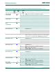
Chapter 10: LPC111x Pin configuration (LPC1100L series, TSSOP, DIP,
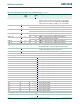
[1] Pin state at reset for default function: I = Input; O = Output; PU = internal pull-up enabled (pins pulled up to full V
DD
level); IA = inactive,
no pull-up/down enabled.
[2] RESET
functionality is not available in Deep power-down mode.
[3] 5 V tolerant pad providing digital I/O functions with configurable pull-up/pull-down resistors and configurable hysteresis.
[4] I
2
C-bus pads compliant with the I
2
C-bus specification for I
2
C standard mode and I
2
C Fast-mode Plus. The pin requires an external
pull-up to provide output functionality. When power is switched off, this pin is floating and does not disturb the I2C lines. Open-drain
configuration applies to all functions on this pin.
[5] 5 V tolerant pad providing digital I/O functions with configurable pull-up/pull-down resistors, configurable hysteresis, and analog input.
When configured as a ADC input, digital section of the pad is disabled and the pin is not 5 V tolerant.
[6] When the system oscillator is not used, connect XTALIN and XTALOUT as follows: XTALIN can be left floating or can be grounded
(grounding is preferred to reduce susceptibility to noise). XTALOUT should be left floating.
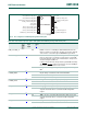
10.3 Pin configuration (LPC1112)
PIO1_7/TXD/
CT32B0_MAT1
12
[3]
no I/O I; PU PIO1_7 — General purpose digital input/output pin.
O- TXD — Transmitter output for UART.
O- CT32B0_MAT1 — Match output 1 for 32-bit timer 0.
V
DD
15 - - 3.3 V supply voltage to the internal regulator, the external rail, and
the ADC. Also used as the ADC reference voltage.
XTALIN 14
[6]
- I - Input to the oscillator circuit and internal clock generator circuits.
Input voltage must not exceed 1.8 V.
XTALOUT 13
[6]
- O - Output from the oscillator amplifier.
V
SS
16 - - Ground.
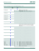
Table 166. LPC1110/11/12 pin description table (SO20 and TSSOP20 package with I
2
C-bus pins) …continued
Symbol
Pin SO20/
TSSOP20
Start
logic
input
Type Reset
state
[1]
Description
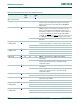
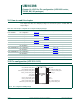
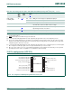
Fig 24. Pin configuration TSSOP20 package with V
DDA
and V
SSA
pins
LPC1112FDH20/102
PIO0_8/MISO0/CT16B0_MAT0 PIO0_3
PIO0_9/MOSI0/CT16B0_MAT1 PIO0_2/SSEL0/CT16B0_CAP0
SWCLK/PIO0_10/SCK0/CT16B0_MAT2 PIO0_1/CLKOUT/CT32B0_MAT2
R/PIO0_11/AD0/CT32B0_MAT3 RESET/PIO0_0
V
DDA
V
SS
V
SSA
V
DD
R/PIO1_0/AD1/CT32B1_CAP0 XTALIN
R/PIO1_1/AD2/CT32B1_MAT0 XTALOUT
R/PIO1_2/AD3/CT32B1_MAT1 PIO1_7/TXD/CT32B0_MAT1
SWDIO/PIO1_3/AD4/CT32B1_MAT2 PIO1_6/RXD/CT32B0_MAT0
002aag597
1
2
3
4
5
6
7
8
9
10
12
11
14
13
16
15
18
17
20
19