
Datasheet


UM10398 All information provided in this document is subject to legal disclaimers. © NXP B.V. 2014. All rights reserved.
User manual Rev. 12.3 — 10 June 2014 172 of 547
NXP Semiconductors
UM10398
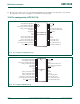
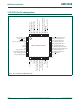
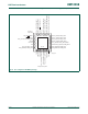
Chapter 10: LPC111x Pin configuration (LPC1100L series, TSSOP, DIP,
[1] Pin state at reset for default function: I = Input; O = Output; PU = internal pull-up enabled (pins pulled up to full V
DD
level); IA = inactive,
no pull-up/down enabled.
[2] RESET
functionality is not available in Deep power-down mode.
[3] 5 V tolerant pad providing digital I/O functions with configurable pull-up/pull-down resistors and configurable hysteresis.
[4] 5 V tolerant pad providing digital I/O functions with configurable pull-up/pull-down resistors, configurable hysteresis, and analog input.
When configured as a ADC input, digital section of the pad is disabled and the pin is not 5 V tolerant.
R/PIO1_0/
AD1/CT32B1_CAP0
7
[4]
yes I I; PU R — Reserved. Configure for an alternate function in the
IOCONFIG block.
I/O - PIO1_0 — General purpose digital input/output pin.
I-AD1 — A/D converter, input 1.
I-CT32B1_CAP0 — Capture input 0 for 32-bit timer 1.
R/PIO1_1/
AD2/CT32B1_MAT0
8
[4]
no O I; PU R — Reserved. Configure for an alternate function in the
IOCONFIG block.
I/O - PIO1_1 — General purpose digital input/output pin.
I-AD2 — A/D converter, input 2.
O-CT32B1_MAT0 — Match output 0 for 32-bit timer 1.
R/PIO1_2/
AD3/CT32B1_MAT1
9
[4]
no I I; PU R — Reserved. Configure for an alternate function in the
IOCONFIG block.
I/O - PIO1_2 — General purpose digital input/output pin.
I-AD3 — A/D converter, input 3.
O-CT32B1_MAT1 — Match output 1 for 32-bit timer 1.
SWDIO/PIO1_3/
AD4/CT32B1_MAT2
10
[4]
no I/O I; PU SWDIO — Serial wire debug input/output.
I/O - PIO1_3 — General purpose digital input/output pin.
I-AD4 — A/D converter, input 4.
O-CT32B1_MAT2 — Match output 2 for 32-bit timer 1.
PIO1_6/RXD/
CT32B0_MAT0
11
[3]
no I/O I; PU PIO1_6 — General purpose digital input/output pin.
I-RXD — Receiver input for UART.
O-CT32B0_MAT0 — Match output 0 for 32-bit timer 0.
PIO1_7/TXD/
CT32B0_MAT1
12
[3]
no I/O I; PU PIO1_7 — General purpose digital input/output pin.
O-TXD — Transmitter output for UART.
O-CT32B0_MAT1 — Match output 1 for 32-bit timer 0.
V
DD
15 - I - 3.3 V supply voltage to the internal regulator and the external
rail.
V
DDA
5 - I - 3.3 V supply voltage to the ADC. Also used as the ADC
reference voltage.
XTALIN 14
[5]
- I - Input to the oscillator circuit and internal clock generator
circuits. Input voltage must not exceed 1.8 V.
XTALOUT 13
[5]
- O - Output from the oscillator amplifier.
V
SS
16 - I - Ground.
V
SSA
6 - I - Analog ground.
Table 167. LPC1112 pin description table (TSSOP20 with V
DDA
and V
SSA
pins) …continued
Symbol
Pin TSSOP20
Start
logic
input
Type Reset
state
[1]
Description