
Datasheet

UM10398 All information provided in this document is subject to legal disclaimers. © NXP B.V. 2014. All rights reserved.
User manual Rev. 12.3 — 10 June 2014 222 of 547
NXP Semiconductors
UM10398
Chapter 13: LPC111x/LPC11Cxx UART
When Auto Direction Control is enabled, the selected pin will be asserted (driven LOW)
when the CPU writes data into the TXFIFO. The pin will be de-asserted (driven HIGH)
once the last bit of data has been transmitted. See bits 4 and 5 in the RS485CTRL
register.
The RS485CTRL bit 4 takes precedence over all other mechanisms controlling the
direction control pin with the exception of loopback mode.
RS485/EIA-485 driver delay time
The driver delay time is the delay between the last stop bit leaving the TXFIFO and the
de-assertion of RTS
. This delay time can be programmed in the 8-bit RS485DLY register.
The delay time is in periods of the baud clock. Any delay time from 0 to 255 bit times may
be used.
RS485/EIA-485 output inversion
The polarity of the direction control signal on the RTS
(or DTR) pins can be reversed by
programming bit 5 in the U0RS485CTRL register. When this bit is set, the direction control
pin will be driven to logic 1 when the transmitter has data waiting to be sent. The direction
control pin will be driven to logic 0 after the last bit of data has been transmitted.
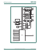
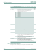
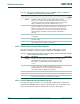
13.6 Architecture
The architecture of the UART is shown below in the block diagram.
The APB interface provides a communications link between the CPU or host and the
UART.
The UART receiver block, U0RX, monitors the serial input line, RXD, for valid input. The
UART RX Shift Register (U0RSR) accepts valid characters via RXD. After a valid
character is assembled in the U0RSR, it is passed to the UART RX Buffer Register FIFO
to await access by the CPU or host via the generic host interface.
The UART transmitter block, U0TX, accepts data written by the CPU or host and buffers
the data in the UART TX Holding Register FIFO (U0THR). The UART TX Shift Register
(U0TSR) reads the data stored in the U0THR and assembles the data to transmit via the
serial output pin, TXD1.
The UART Baud Rate Generator block, U0BRG, generates the timing enables used by the
UART TX block. The U0BRG clock input source is UART_PCLK. The main clock is
divided down per the divisor specified in the U0DLL and U0DLM registers. This divided
down clock is a 16x oversample clock, NBAUDOUT.
The interrupt interface contains registers U0IER and U0IIR. The interrupt interface
receives several one clock wide enables from the U0TX and U0RX blocks.
Status information from the U0TX and U0RX is stored in the U0LSR. Control information
for the U0TX and U0RX is stored in the U0LCR.