
Datasheet

UM10398 All information provided in this document is subject to legal disclaimers. © NXP B.V. 2014. All rights reserved.
User manual Rev. 12.3 — 10 June 2014 233 of 547
NXP Semiconductors
UM10398
Chapter 14: LPC111x/LPC11Cxx SPI0/1 with SSP
The CPHA control bit selects the clock edge that captures data and allows it to change
state. It has the most impact on the first bit transmitted by either allowing or not allowing a
clock transition before the first data capture edge. When the CPHA phase control bit is
LOW, data is captured on the first clock edge transition. If the CPHA clock phase control
bit is HIGH, data is captured on the second clock edge transition.
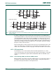
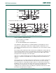
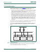
14.7.2.2 SPI format with CPOL=0,CPHA=0
Single and continuous transmission signal sequences for SPI format with CPOL = 0,
CPHA = 0 are shown in Figure 38
.
In this configuration, during idle periods:
• The CLK signal is forced LOW.
• SSEL is forced HIGH.
• The transmit MOSI/MISO pad is in high impedance.
If the SPI/SSP is enabled and there is valid data within the transmit FIFO, the start of
transmission is signified by the SSEL master signal being driven LOW. This causes slave
data to be enabled onto the MISO input line of the master. Master’s MOSI is enabled.
One half SCK period later, valid master data is transferred to the MOSI pin. Now that both
the master and slave data have been set, the SCK master clock pin goes HIGH after one
further half SCK period.
The data is captured on the rising and propagated on the falling edges of the SCK signal.
a. Single transfer with CPOL=0 and CPHA=0
b. Continuous transfer with CPOL=0 and CPHA=0
Fig 38. SPI frame format with CPOL=0 and CPHA=0 (a) Single and b) Continuous Transfer)
SCK
SSEL
MOSI
MSB LSB
QMSB LSB
4 to 16 bits
MISO
SCK
SSEL
MOSI
MISO
4 to 16 bits
4 to 16 bits
MSB LSBMSB LSB
QMSB LSB QMSB LSB