
Datasheet


UM10398 All information provided in this document is subject to legal disclaimers. © NXP B.V. 2014. All rights reserved.
User manual Rev. 12.3 — 10 June 2014 254 of 547
NXP Semiconductors
UM10398
Chapter 15: LPC111x/LPC11Cxx I2C-bus controller
15.9.2 Address Registers, ADDR0 to ADDR3
These registers may be loaded with the 7-bit slave address (7 most significant bits) to
which the I
2
C block will respond when programmed as a slave transmitter or receiver. The
LSB (GC) is used to enable General Call address (0x00) recognition. When multiple slave
addresses are enabled, the actual address received may be read from the DAT register at
the state where the own slave address has been received.
15.9.3 Address mask registers, MASK0 to MASK3
The four mask registers each contain seven active bits (7:1). Any bit in these registers
which is set to ‘1’ will cause an automatic compare on the corresponding bit of the
received address when it is compared to the ADDRn register associated with that mask
register. In other words, bits in an ADDRn register which are masked are not taken into
account in determining an address match.
When an address-match interrupt occurs, the processor will have to read the data register
(DAT) to determine what the received address was that actually caused the match.
15.9.4 Comparator
The comparator compares the received 7-bit slave address with its own slave address (7
most significant bits in ADR). It also compares the first received 8-bit byte with the General
Call address (0x00). If an equality is found, the appropriate status bits are set and an
interrupt is requested.
15.9.5 Shift register, DAT
This 8-bit register contains a byte of serial data to be transmitted or a byte which has just
been received. Data in DAT is always shifted from right to left; the first bit to be transmitted
is the MSB (bit 7) and, after a byte has been received, the first bit of received data is
located at the MSB of DAT. While data is being shifted out, data on the bus is
simultaneously being shifted in; DAT always contains the last byte present on the bus.
Thus, in the event of lost arbitration, the transition from master transmitter to slave
receiver is made with the correct data in DAT.
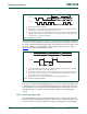
15.9.6 Arbitration and synchronization logic
In the master transmitter mode, the arbitration logic checks that every transmitted logic 1
actually appears as a logic 1 on the I
2
C-bus. If another device on the bus overrules a logic
1 and pulls the SDA line low, arbitration is lost, and the I
2
C block immediately changes
from master transmitter to slave receiver. The I
2
C block will continue to output clock
pulses (on SCL) until transmission of the current serial byte is complete.
Arbitration may also be lost in the master receiver mode. Loss of arbitration in this mode
can only occur while the I
2
C block is returning a “not acknowledge: (logic 1) to the bus.
Arbitration is lost when another device on the bus pulls this signal low. Since this can
occur only at the end of a serial byte, the I
2
C block generates no further clock pulses.
Figure 52
shows the arbitration procedure.