
Datasheet

UM10398 All information provided in this document is subject to legal disclaimers. © NXP B.V. 2014. All rights reserved.
User manual Rev. 12.3 — 10 June 2014 35 of 547
NXP Semiconductors
UM10398
Chapter 3: LPC111x/LPC11Cxx System configuration (SYSCON)
3.5.18 WDT clock source select register
This register selects the clock source for the watchdog timer. The WDTCLKUEN register
(see Section 3.5.19
) must be toggled from LOW to HIGH for the update to take effect.
Remark: When switching clock sources, both clocks must be running before the clock
source is updated.
3.5.19 WDT clock source update enable register
This register updates the clock source of the watchdog timer with the new input clock after
the WDTCLKSEL register has been written to. In order for the update to take effect at the
input of the watchdog timer, first write a zero to the WDTCLKUEN register and then write
a one to WDTCLKUEN.
Remark: When switching clock sources, both clocks must be running before the clock
source is updated.
3.5.20 WDT clock divider register
This register determines the divider values for the watchdog clock wdt_clk.
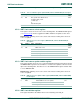
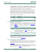
Table 24. SPI1 clock divider register (SSP1CLKDIV, address 0x4004 809C) bit description
Bit Symbol Description Reset
value
7:0 DIV SPI1_PCLK clock divider values
0: Disable SPI1_PCLK.
1: Divide by 1.
to
255: Divide by 255.
0x00
31:8 - Reserved 0x00
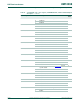
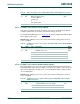
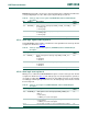
Table 25. WDT clock source select register (WDTCLKSEL, address 0x4004 80D0) bit
description
Bit Symbol Value Description Reset
value
1:0 SEL WDT clock source 0x00
0x0 IRC oscillator
0x1 Main clock
0x2 Watchdog oscillator
0x3 Reserved
31:2 - - Reserved 0x00
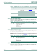
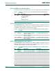
Table 26. WDT clock source update enable register (WDTCLKUEN, address 0x4004 80D4)
bit description
Bit Symbol Value Description Reset value
0 ENA Enable WDT clock source update 0x0
0 No change
1 Update clock source
31:1 - - Reserved 0x00