
Datasheet


UM10398 All information provided in this document is subject to legal disclaimers. © NXP B.V. 2014. All rights reserved.
User manual Rev. 12.3 — 10 June 2014 378 of 547
NXP Semiconductors
UM10398
Chapter 21: LPC1100XL series: 32-bit counter/timer CT32B0/1
[1] Reset value reflects the data stored in used bits only. It does not include reserved bits content.
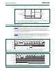
Table 328. Register overview: 32-bit counter/timer 0 CT32B0 (base address 0x4001 4000)
Name Access Address
offset
Description Reset
value
[1]
TMR32B0IR R/W 0x000 Interrupt Register (IR). The IR can be written to clear interrupts. The IR
can be read to identify which of five possible interrupt sources are
pending.
0
TMR32B0TCR R/W 0x004 Timer Control Register (TCR). The TCR is used to control the Timer
Counter functions. The Timer Counter can be disabled or reset through
the TCR.
0
TMR32B0TC R/W 0x008 Timer Counter (TC). The 32-bit TC is incremented every PR+1 cycles of
PCLK. The TC is controlled through the TCR.
0
TMR32B0PR R/W 0x00C Prescale Register (PR). When the Prescale Counter (below) is equal to
this value, the next clock increments the TC and clears the PC.
0
TMR32B0PC R/W 0x010 Prescale Counter (PC). The 32-bit PC is a counter which is incremented
to the value stored in PR. When the value in PR is reached, the TC is
incremented and the PC is cleared. The PC is observable and
controllable through the bus interface.
0
TMR32B0MCR R/W 0x014 Match Control Register (MCR). The MCR is used to control if an
interrupt is generated and if the TC is reset when a Match occurs.
0
TMR32B0MR0 R/W 0x018 Match Register 0 (MR0). MR0 can be enabled through the MCR to reset
the TC, stop both the TC and PC, and/or generate an interrupt every
time MR0 matches the TC.
0
TMR32B0MR1 R/W 0x01C Match Register 1 (MR1). See MR0 description. 0
TMR32B0MR2 R/W 0x020 Match Register 2 (MR2). See MR0 description. 0
TMR32B0MR3 R/W 0x024 Match Register 3 (MR3). See MR0 description. 0
TMR32B0CCR R/W 0x028 Capture Control Register (CCR). The CCR controls which edges of the
capture inputs are used to load the Capture Registers and whether or
not an interrupt is generated when a capture takes place.
0
TMR32B0CR0 RO 0x02C Capture Register 0 (CR0). CR0 is loaded with the value of TC when
there is an event on the CT32B0_CAP0 input.
0
TMR32B0CR1 RO 0x030 Capture Register 1 (CR1). CR1 is loaded with the value of TC when
there is an event on the CT32B0_CAP1 input.
0
- - 0x034 -
0x038
Reserved -
TMR32B0EMR R/W 0x03C External Match Register (EMR). The EMR controls the match function
and the external match pins CT32B0_MAT[3:0].
0
- - 0x040 -
0x06C
Reserved -
TMR32B0CTCR R/W 0x070 Count Control Register (CTCR). The CTCR selects between Timer and
Counter mode, and in Counter mode selects the signal and edge(s) for
counting.
0
TMR32B0PWMC R/W 0x074 PWM Control Register (PWMCON). The PWMCON enables PWM
mode for the external match pins CT32B0_MAT[3:0].
0