
Datasheet

UM10398 All information provided in this document is subject to legal disclaimers. © NXP B.V. 2014. All rights reserved.
User manual Rev. 12.3 — 10 June 2014 74 of 547
NXP Semiconductors
UM10398
Chapter 7: LPC1100/LPC1100C/LPC1100L series: I/O configuration
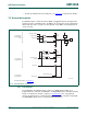
7.3.6 Open-drain Mode
When output is selected, either by selecting a special function in the FUNC field, or by
selecting GPIO function for a pin having a 1 in its GPIODIR register, a 1 in the OD bit
selects open-drain operation, that is, a 1 disables the high-drive transistor. This option has
no effect on the primary I
2
C pins.
Remark: The open-drain mode is not available on all parts (see Section 7.1
).
7.4 Register description
The I/O configuration registers control the PIO port pins, the inputs and outputs of all
peripherals and functional blocks, the I
2
C-bus pins, and the ADC input pins.
Each port pin PIOn_m has one IOCON register assigned to control the pin’s function and
electrical characteristics.
Some input functions (SCK0, DSR
, DCD, and RI) are multiplexed to several physical pins.
The IOCON_LOC registers select the pin location for each of these functions.
Remark: The IOCON registers are listed in order of their memory locations in Table 56
,
which correspond to the order of their physical pin numbers in the LQFP48 package
starting at the upper left corner with pin 1 (PIO2_6). See Table 57
for a listing of IOCON
registers ordered by port number.
The IOCON location registers are used to select a physical pin for multiplexed functions.
Remark: Note that once the pin location has been selected, the function still must be
configured in the corresponding IOCON registers for the function to be usable on that pin.
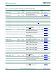
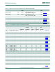
Table 56. Register overview: I/O configuration (base address 0x4004 4000)
Name Access Address
offset
Description Reset
value
Reference
IOCON_PIO2_6 R/W 0x000 I/O configuration for pin PIO2_6 0xD0 Table 58
- R/W 0x004 Reserved - -
IOCON_PIO2_0 R/W 0x008 I/O configuration for pin
PIO2_0/DTR
/SSEL1
0xD0 Ta ble 59
IOCON_RESET_PIO0_0 R/W 0x00C I/O configuration for pin RESET/PIO0_0 0xD0 Table 60
IOCON_PIO0_1 R/W 0x010 I/O configuration for pin
PIO0_1/CLKOUT/CT32B0_MAT2
0xD0 Ta ble 61
IOCON_PIO1_8 R/W 0x014 I/O configuration for pin
PIO1_8/CT16B1_CAP0
0xD0 Ta ble 62
- R/W 0x018 Reserved - -
IOCON_PIO0_2 R/W 0x01C I/O configuration for pin
PIO0_2/SSEL0/CT16B0_CAP0
0xD0 Ta ble 63
IOCON_PIO2_7 R/W 0x020 I/O configuration for pin PIO2_7 0xD0 Table 64
IOCON_PIO2_8 R/W 0x024 I/O configuration for pin PIO2_8 0xD0 Table 65
IOCON_PIO2_1 R/W 0x028 I/O configuration for pin
PIO2_1/DSR/
SCK1
0xD0 Ta ble 66
IOCON_PIO0_3 R/W 0x02C I/O configuration for pin PIO0_3 0xD0 Table 67
IOCON_PIO0_4 R/W 0x030 I/O configuration for pin PIO0_4/SCL 0x00 Table 68