
Datasheet


LPC111X All information provided in this document is subject to legal disclaimers. © NXP Semiconductors N.V. 2014. All rights reserved.
Product data sheet Rev. 9.2 — 26 March 2014 19 of 127
NXP Semiconductors
LPC1110/11/12/13/14/15
32-bit ARM Cortex-M0 microcontroller
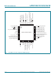
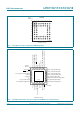
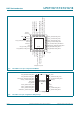
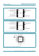
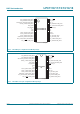
6.2 Pin description
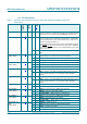
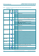
Table 4. LPC1100L series: LPC1110/11/12 pin description table (SO20 and TSSOP20 package with
I
2
C-bus pins)
Symbol
Pin SO20/
TSSOP20
Start
logic
input
Type Reset
state
[1]
Description
PIO0_0 to PIO0_11 I/O Port 0 — Port 0 is a 12-bit I/O port with individual direction and
function controls for each bit. The operation of port 0 pins depends
on the function selected through the IOCONFIG register block.
RESET
/PIO0_0 17
[2]
yes I I; PU RESET — External reset input with 20 ns glitch filter. A LOW-going
pulse as short as 50 ns on this pin resets the device, causing I/O
ports and peripherals to take on their default states, and processor
execution to begin at address 0.
In deep power-down mode, this pin must be pulled HIGH externally.
The RESET
pin can be left unconnected or be used as a GPIO pin
if an external RESET function is not needed and Deep power-down
mode is not used.
I/O - PIO0_0 — General purpose digital input/output pin with 10 ns glitch
filter.
PIO0_1/CLKOUT/
CT32B0_MAT2
18
[3]
yes I/O I; PU PIO0_1 — General purpose digital input/output pin. A LOW level on
this pin during reset starts the ISP command handler.
O- CLKOUT — Clockout pin.
O- CT32B0_MAT2 — Match output 2 for 32-bit timer 0.
PIO0_2/SSEL0/
CT16B0_CAP0
19
[3]
yes I/O I; PU PIO0_2 — General purpose digital input/output pin.
I/O - SSEL0 — Slave Select for SPI0.
I- CT16B0_CAP0 — Capture input 0 for 16-bit timer 0.
PIO0_4/SCL 20
[4]
yes I/O I; IA PIO0_4 — General purpose digital input/output pin (open-drain).
I/O - SCL — I
2
C-bus, open-drain clock input/output. High-current sink
only if I
2
C Fast-mode Plus is selected in the I/O configuration
register.
PIO0_5/SDA 5
[4]
yes I/O I; IA PIO0_5 — General purpose digital input/output pin (open-drain).
I/O - SDA — I
2
C-bus, open-drain data input/output. High-current sink
only if I
2
C Fast-mode Plus is selected in the I/O configuration
register.
PIO0_6/SCK0 6
[3]
yes I/O I; PU PIO0_6 — General purpose digital input/output pin.
I/O - SCK0 — Serial clock for SPI0.
PIO0_8/MISO0/
CT16B0_MAT0
1
[3]
yes I/O I; PU PIO0_8 — General purpose digital input/output pin.
I/O - MISO0 — Master In Slave Out for SPI0.
O- CT16B0_MAT0 — Match output 0 for 16-bit timer 0.
PIO0_9/MOSI0/
CT16B0_MAT1
2
[3]
yes I/O I; PU PIO0_9 — General purpose digital input/output pin.
I/O - MOSI0 — Master Out Slave In for SPI0.
O- CT16B0_MAT1 — Match output 1 for 16-bit timer 0.
SWCLK/PIO0_10/
SCK0/
CT16B0_MAT2
3
[3]
yes I I; PU SWCLK — Serial wire clock.
I/O - PIO0_10 — General purpose digital input/output pin.
I/O - SCK0 — Serial clock for SPI0.
O- CT16B0_MAT2 — Match output 2 for 16-bit timer 0.