
Datasheet

LPC111X All information provided in this document is subject to legal disclaimers. © NXP Semiconductors N.V. 2014. All rights reserved.
Product data sheet Rev. 9.2 — 26 March 2014 24 of 127
NXP Semiconductors
LPC1110/11/12/13/14/15
32-bit ARM Cortex-M0 microcontroller
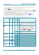
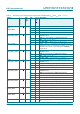
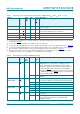
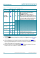
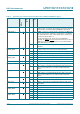
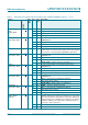
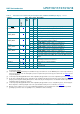
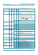
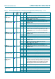
PIO0_5/SDA 9
[4]
yes I/O I; IA PIO0_5 — General purpose digital input/output pin
(open-drain).
I/O - SDA — I
2
C-bus, open-drain data input/output. High-current
sink only if I
2
C Fast-mode Plus is selected in the I/O
configuration register.
PIO0_6/SCK0 10
[3]
yes I/O I; PU PIO0_6 — General purpose digital input/output pin.
I/O - SCK0 — Serial clock for SPI0.
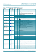
PIO0_7/CTS
11
[3]
yes I/O I; PU PIO0_7 — General purpose digital input/output pin
(high-current output driver).
I-CTS
— Clear To Send input for UART.
PIO0_8/MISO0/
CT16B0_MAT0
12
[3]
yes I/O I; PU PIO0_8 — General purpose digital input/output pin.
I/O - MISO0 — Master In Slave Out for SPI0.
O-CT16B0_MAT0 — Match output 0 for 16-bit timer 0.
PIO0_9/MOSI0/
CT16B0_MAT1
13
[3]
yes I/O I; PU PIO0_9 — General purpose digital input/output pin.
I/O - MOSI0 — Master Out Slave In for SPI0.
O-CT16B0_MAT1 — Match output 1 for 16-bit timer 0.
SWCLK/PIO0_10/
SCK0/
CT16B0_MAT2
14
[3]
yes I I; PU SWCLK — Serial wire clock.
I/O - PIO0_10 — General purpose digital input/output pin.
I/O - SCK0 — Serial clock for SPI0.
O-CT16B0_MAT2 — Match output 2 for 16-bit timer 0.
R/PIO0_11/
AD0/CT32B0_MAT3
15
[5]
yes I I; PU R — Reserved. Configure for an alternate function in the
IOCONFIG block.
I/O - PIO0_11 — General purpose digital input/output pin.
I-AD0 — A/D converter, input 0.
O-CT32B0_MAT3 — Match output 3 for 32-bit timer 0.
R/PIO1_0/
AD1/CT32B1_CAP0
16
[5]
yes I I; PU R — Reserved. Configure for an alternate function in the
IOCONFIG block.
I/O - PIO1_0 — General purpose digital input/output pin.
I-AD1 — A/D converter, input 1.
I-CT32B1_CAP0 — Capture input 0 for 32-bit timer 1.
R/PIO1_1/
AD2/CT32B1_MAT0
17
[5]
no O I; PU R — Reserved. Configure for an alternate function in the
IOCONFIG block.
I/O - PIO1_1 — General purpose digital input/output pin.
I-AD2 — A/D converter, input 2.
O-CT32B1_MAT0 — Match output 0 for 32-bit timer 1.
R/PIO1_2/
AD3/CT32B1_MAT1
18
[5]
no I I; PU R — Reserved. Configure for an alternate function in the
IOCONFIG block.
I/O - PIO1_2 — General purpose digital input/output pin.
I-AD3 — A/D converter, input 3.
O-CT32B1_MAT1 — Match output 1 for 32-bit timer 1.
Table 6. LPC1100L series: LPC1112 (HVQFN24 package)
…continued
Symbol HVQFN
pin
Start
logic
input
Type Reset
state
[1]
Description