
Datasheet

LPC111X All information provided in this document is subject to legal disclaimers. © NXP Semiconductors N.V. 2014. All rights reserved.
Product data sheet Rev. 9.2 — 26 March 2014 30 of 127
NXP Semiconductors
LPC1110/11/12/13/14/15
32-bit ARM Cortex-M0 microcontroller
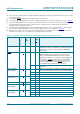
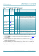
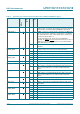
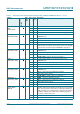
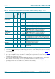
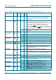
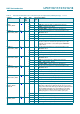
SWCLK/PIO0_10/
SCK0/
CT16B0_MAT2
29
[3]
yes I I; PU SWCLK — Serial wire clock.
I/O - PIO0_10 — General purpose digital input/output pin.
I/O - SCK0 — Serial clock for SPI0.
O-CT16B0_MAT2 — Match output 2 for 16-bit timer 0.
R/PIO0_11/
AD0/CT32B0_MAT3
32
[5]
yes I I; PU R — Reserved. Configure for an alternate function in the
IOCONFIG block.
I/O - PIO0_11 — General purpose digital input/output pin.
I-AD0 — A/D converter, input 0.
O-CT32B0_MAT3 — Match output 3 for 32-bit timer 0.
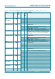
PIO1_0 to PIO1_11 I/O Port 1 — Port 1 is a 12-bit I/O port with individual direction and
function controls for each bit. The operation of port 1 pins
depends on the function selected through the IOCONFIG
register block.
R/PIO1_0/
AD1/CT32B1_CAP0
33
[5]
yes I I; PU R — Reserved. Configure for an alternate function in the
IOCONFIG block.
I/O - PIO1_0 — General purpose digital input/output pin.
I-AD1 — A/D converter, input 1.
I-CT32B1_CAP0 — Capture input 0 for 32-bit timer 1.
R/PIO1_1/
AD2/CT32B1_MAT0
34
[5]
no O I; PU R — Reserved. Configure for an alternate function in the
IOCONFIG block.
I/O - PIO1_1 — General purpose digital input/output pin.
I-AD2 — A/D converter, input 2.
O-CT32B1_MAT0 — Match output 0 for 32-bit timer 1.
R/PIO1_2/
AD3/CT32B1_MAT1
35
[5]
no I I; PU R — Reserved. Configure for an alternate function in the
IOCONFIG block.
I/O - PIO1_2 — General purpose digital input/output pin.
I-AD3 — A/D converter, input 3.
O-CT32B1_MAT1 — Match output 1 for 32-bit timer 1.
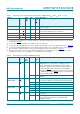
SWDIO/PIO1_3/
AD4/CT32B1_MAT2
39
[5]
no I/O I; PU SWDIO — Serial wire debug input/output.
I/O - PIO1_3 — General purpose digital input/output pin.
I-AD4 — A/D converter, input 4.
O-CT32B1_MAT2 — Match output 2 for 32-bit timer 1.
PIO1_4/AD5/
CT32B1_MAT3/
WAKEUP
40
[5]
no I/O I; PU PIO1_4 — General purpose digital input/output pin with 10 ns
glitch filter. In Deep power-down mode, this pin serves as the
Deep power-down mode wake-up pin with 20 ns glitch filter. Pull
this pin HIGH externally before entering Deep power-down
mode. Pull this pin LOW to exit Deep power-down mode. A
LOW-going pulse as short as 50 ns wakes up the part.
I-AD5 — A/D converter, input 5.
O-CT32B1_MAT3 — Match output 3 for 32-bit timer 1.
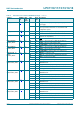
PIO1_5/RTS
/
CT32B0_CAP0
45
[3]
no I/O I; PU PIO1_5 — General purpose digital input/output pin.
O-RTS
— Request To Send output for UART.
I-CT32B0_CAP0 — Capture input 0 for 32-bit timer 0.
Table 8. LPC1100 and LPC1100L series: LPC1113/14 pin description table (LQFP48 package) …continued
Symbol Pin Start
logic
input
Type Reset
state
[1]
Description