
Datasheet


LPC111X All information provided in this document is subject to legal disclaimers. © NXP Semiconductors N.V. 2014. All rights reserved.
Product data sheet Rev. 9.2 — 26 March 2014 56 of 127
NXP Semiconductors
LPC1110/11/12/13/14/15
32-bit ARM Cortex-M0 microcontroller
The start logic must be configured in the system configuration block and in the NVIC
before being used.
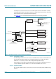
7.17.2 Reset
Reset has four sources on the LPC1110/11/12/13/14/15: the RESET pin, the Watchdog
reset, Power-On Reset (POR), and the BrownOut Detection (BOD) circuit. The RESET
pin is a Schmitt trigger input pin. Assertion of chip reset by any source, once the operating
voltage attains a usable level, starts the IRC and initializes the flash controller.
A LOW-going pulse as short as 50 ns resets the part.
When the internal Reset is removed, the processor begins executing at address 0, which
is initially the Reset vector mapped from the boot block. At that point, all of the processor
and peripheral registers have been initialized to predetermined values.
An external pull-up resistor is required on the RESET
pin if Deep power-down mode is
used.
7.17.3 Brownout detection
The LPC1110/11/12/13/14/15 includes up to four levels for monitoring the voltage on the
V
DD
pin. If this voltage falls below one of the selected levels, the BOD asserts an interrupt
signal to the NVIC. This signal can be enabled for interrupt in the Interrupt Enable
Register in the NVIC in order to cause a CPU interrupt; if not, software can monitor the
signal by reading a dedicated status register. Four threshold levels can be selected to
cause a forced reset of the chip.
7.17.4 Code security (Code Read Protection - CRP)
This feature of the LPC1110/11/12/13/14/15 allows user to enable different levels of
security in the system so that access to the on-chip flash and use of the Serial Wire
Debugger (SWD) and In-System Programming (ISP) can be restricted. When needed,
CRP is invoked by programming a specific pattern into a dedicated flash location. IAP
commands are not affected by the CRP.
In addition, ISP entry via the PIO0_1 pin can be disabled without enabling CRP. For
details see the LPC111x user manual.
There are three levels of Code Read Protection:
1. CRP1 disables access to the chip via the SWD and allows partial flash update
(excluding flash sector 0) using a limited set of the ISP commands. This mode is
useful when CRP is required and flash field updates are needed but all sectors can
not be erased.
2. CRP2 disables access to the chip via the SWD and only allows full flash erase and
update using a reduced set of the ISP commands.
3. Running an application with level CRP3 selected fully disables any access to the chip
via the SWD pins and the ISP. This mode effectively disables ISP override using
PIO0_1 pin, too. It is up to the user’s application to provide (if needed) flash update
mechanism using IAP calls or call reinvoke ISP command to enable flash update via
the UART.