LPC2104/2105/2106 Single-chip 32-bit microcontrollers; 128 kB ISP/IAP flash with 16/32/64 kB RAM Rev. 07 — 20 June 2008 Product data sheet 1. General description The UART are based on a 16/32-bit ARM7TDMI-S CPU with real-time emulation and embedded trace support, together with 128 kB of embedded high speed flash memory. A 128-bit wide memory interface and a unique accelerator architecture enable 32-bit code execution at maximum clock rate.
LPC2104/2105/2106 NXP Semiconductors Single-chip 32-bit microcontrollers n In-System Programming (ISP) and In-Application Programming (IAP) via on-chip bootloader software. Flash programming takes 1 ms per 512 B line. Single sector or full chip erase takes 400 ms. n Vectored Interrupt Controller with configurable priorities and vector addresses. n EmbeddedICE-RT interface enables breakpoints and watch points.
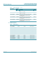
LPC2104/2105/2106 NXP Semiconductors Single-chip 32-bit microcontrollers Table 1. Ordering information …continued Type number Package Name Description Version LPC2106FBD48/00 LQFP48 plastic low profile quad flat package; 48 leads; body 7 × 7 × 1.4 mm SOT313-2 LPC2106FBD48/01 LQFP48 plastic low profile quad flat package; 48 leads; body 7 × 7 × 1.4 mm SOT313-2 LPC2106FHN48 HVQFN48 plastic thermal enhanced very thin quad flat package; no leads; 48 terminals; body 7 × 7 × 0.
LPC2104/2105/2106 NXP Semiconductors Single-chip 32-bit microcontrollers 4.
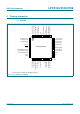
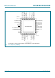
LPC2104/2105/2106 NXP Semiconductors Single-chip 32-bit microcontrollers 5. Pinning information 37 P0.12/DSR1/MAT1.0 38 P0.25/PIPESTAT2 39 P0.26/TRACESYNC 40 VDD(3V3) 41 P0.13/DTR1/MAT1.1 43 VSS 42 n.c. 44 P0.14/DCD1/EINT1 45 P0.15/RI1/EINT2 46 P0.16/EINT0/MAT0.2 47 P0.17/CAP1.2/TRST 48 P0.18/CAP1.3/TMS 5.1 Pinning P0.19/MAT1.2/TCK 1 36 P0.11/CTS1/CAP1.1 P0.20/MAT1.3/TDI 2 35 P0.10/RTS1/CAP1.0 P0.21/PWM5/TDO 3 34 P0.24/PIPESTAT1 n.c. 4 33 P0.23/PIPESTAT0 VDD(1V8) 5 32 P0.
LPC2104/2105/2106 NXP Semiconductors 37 P0.12/DSR1/MAT1.0 38 P0.25/PIPESTAT2 40 VDD(3V3) 39 P0.26/TRACESYNC 41 P0.13/DTR1/MAT1.1 43 VSS 42 n.c. 44 P0.14/DCD1/EINT1 45 P0.15/RI1/EINT2 46 P0.16/EINT0/MAT0.2 terminal 1 index area 47 P0.17/CAP1.2/TRST 48 P0.18/CAP1.3/TMS Single-chip 32-bit microcontrollers P0.19/MAT1.2/TCK 1 36 P0.11/CTS1/CAP1.1 P0.20/MAT1.3/TDI 2 35 P0.10/RTS1/CAP1.0 P0.21/PWM5/TDO 3 34 P0.24/PIPESTAT1 n.c. 4 33 P0.23/PIPESTAT0 VDD(1V8) 5 32 P0.
LPC2104/2105/2106 NXP Semiconductors Single-chip 32-bit microcontrollers 5.2 Pin description Table 3. Pin description Symbol Pin P0.0 to P0.31 P0.0/TXD0/PWM1 P0.1/RXD0/PWM3 P0.2/SCL/CAP0.0 P0.3/SDA/MAT0.0 P0.4/SCK/CAP0.1 P0.5/MISO/MAT0.1 P0.6/MOSI/CAP0.2 P0.7/SSEL/PWM2 P0.8/TXD1/PWM4 P0.9/RXD1/PWM6 P0.10/RTS1/CAP1.
LPC2104/2105/2106 NXP Semiconductors Single-chip 32-bit microcontrollers Table 3. Pin description …continued Symbol Pin Type Description P0.11/CTS1/CAP1.1 36[1] I/O P0.11 — Port 0 bit 11. I CTS1 — Clear to Send input for UART 1. I CAP1.1 — Capture input for Timer 1, channel 1. I/O P0.12 — Port 0 bit 12. I DSR1 — Data Set Ready input for UART 1. O MAT1.0 — Match output for Timer 1, channel 0. I/O P0.13 — Port 0 bit 13. O DTR1 — Data Terminal Ready output for UART 1. O MAT1.
LPC2104/2105/2106 NXP Semiconductors Single-chip 32-bit microcontrollers Table 3. Pin description …continued Symbol Pin Type Description P0.26/TRACESYNC 39[4] I/O P0.26 — Port 0 bit 26. O TRACESYNC — Trace Synchronization Standard I/O port with internal pull-up. P0.27/TRACEPKT0/ TRST 8[4] I/O P0.27 — Port 0 bit 27. O TRACEPKT0 — Trace Packet, bit 0. Standard I/O port with internal pull-up. I TRST — Test Reset for JTAG interface, secondary JTAG pin group. I/O P0.28 — Port 0 bit 28.
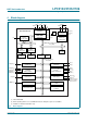
LPC2104/2105/2106 NXP Semiconductors Single-chip 32-bit microcontrollers 6. Functional description 6.1 Architectural overview The ARM7TDMI-S is a general purpose 32-bit microprocessor, which offers high performance and very low power consumption. The ARM architecture is based on Reduced Instruction Set Computer (RISC) principles, and the instruction set and related decode mechanism are much simpler than those of microprogrammed Complex Instruction Set Computers.
LPC2104/2105/2106 NXP Semiconductors Single-chip 32-bit microcontrollers 6.4 Memory map The LPC2104/2105/2106 memory maps incorporate several distinct regions, as shown in the following figures. In addition, the CPU interrupt vectors may be re-mapped to allow them to reside in either flash memory (the default) or on-chip static RAM. This is described in Section 6.18 “System control”. 4.0 GB 0xFFFF FFFF AHB PERIPHERALS 3.75 GB APB PERIPHERALS 0xF000 0000 0xEFFF FFFF 0xE000 0000 0xDFFF FFFF 3.
LPC2104/2105/2106 NXP Semiconductors Single-chip 32-bit microcontrollers 6.5 Interrupt controller The Vectored Interrupt Controller (VIC) accepts all of the Interrupt Request (IRQ) inputs and categorizes, them as FIQ, vectored IRQ, and non-vectored IRQ as defined by programmable settings. The programmable assignment scheme means that priorities of interrupts from the various peripherals can be dynamically assigned and adjusted. Fast Interrupt reQuest (FIQ) has the highest priority.
LPC2104/2105/2106 NXP Semiconductors Single-chip 32-bit microcontrollers Table 4.
LPC2104/2105/2106 NXP Semiconductors Single-chip 32-bit microcontrollers Table 6. Pin function select register 0 (PINSEL0 - 0xE002 C000) PINSEL0 Pin name Value 1:0 P0.0 0 3:2 5:4 7:6 9:8 11:10 13:12 15:14 17:16 19:18 21:20 23:22 25:24 P0.1 P0.2 P0.3 P0.4 P0.5 P0.6 P0.7 P0.8 P0.9 P0.10 P0.11 P0.12 Function Value after reset 0 GPIO Port 0.0 0 0 1 TXD (UART 0) 1 0 PWM1 0 0 GPIO Port 0.1 0 1 RXD (UART 0) 1 0 PWM3 0 0 GPIO Port 0.
LPC2104/2105/2106 NXP Semiconductors Single-chip 32-bit microcontrollers Table 6. Pin function select register 0 (PINSEL0 - 0xE002 C000) …continued PINSEL0 Pin name Value Function Value after reset 27:26 P0.13 0 0 GPIO Port 0.13 0 0 1 DTR (UART 1) 1 0 Match 1.1 (Timer 1) 29:28 31:30 P0.14 P0.15 0 0 GPIO Port 0.14 0 1 DCD (UART 1) 1 0 EINT1 0 0 GPIO Port 0.15 0 1 RI (UART 1) 1 0 EINT2 0 0 6.
LPC2104/2105/2106 NXP Semiconductors Single-chip 32-bit microcontrollers Table 7. Pin function select register 1 (PINSEL1 - 0xE002 C004) …continued PINSEL1 Pin name Value 25:24 P0.28 0 0 27:26 29:28 31:30 P0.29 P0.30 P0.31 Function Value after reset 0 GPIO Port 0.28 0 1 TMS 0 0 GPIO Port 0.29 0 1 TCK 0 0 GPIO Port 0.30 0 1 TDI 0 0 GPIO Port 0.31 0 1 TDO 0 0 0 6.
LPC2104/2105/2106 NXP Semiconductors Single-chip 32-bit microcontrollers • Standard modem interface signals included on UART 1. 6.10.2 UART features available in LPC2104/2105/2106/01 only Compared to previous LPC2000 microcontrollers, UARTs in LPC2104/2105/2106/01 introduce a fractional baud rate generator for both UARTs, enabling these microcontrollers to achieve standard baud rates such as 115200 Bd with any crystal frequency above 2 MHz.
LPC2104/2105/2106 NXP Semiconductors Single-chip 32-bit microcontrollers 6.12 SPI serial I/O controller The SPI is a full duplex serial interface, designed to be able to handle multiple masters and slaves connected to a given bus. Only a single master and a single slave can communicate on the interface during a given data transfer. During a data transfer the master always sends a byte of data to the slave, and the slave always sends a byte of data to the master. 6.12.
LPC2104/2105/2106 NXP Semiconductors Single-chip 32-bit microcontrollers 6.14.1 Features • A 32-bit Timer/Counter with a programmable 32-bit Prescaler. • Up to four (Timer 1) and three (Timer 0) 32-bit capture channels, that can take a snapshot of the timer value when an input signal transitions. A capture event may also optionally generate an interrupt. • Four 32-bit match registers that allow: – Continuous operation with optional interrupt generation on match.
LPC2104/2105/2106 NXP Semiconductors Single-chip 32-bit microcontrollers • Programmable 32-bit timer with internal pre-scaler. • Selectable time period from (Tcy(PCLK) × 256 × 4) to (Tcy(PCLK) × 232 × 4) in multiples of Tcy(PCLK) × 4. 6.16 Real time clock The Real Time Clock (RTC) is designed to provide a set of counters to measure time when normal or idle operating mode is selected.
LPC2104/2105/2106 NXP Semiconductors Single-chip 32-bit microcontrollers With double edge controlled PWM outputs, specific match registers control the rising and falling edge of the output. This allows both positive going PWM pulses (when the rising edge occurs prior to the falling edge), and negative going PWM pulses (when the falling edge occurs prior to the rising edge). 6.17.
LPC2104/2105/2106 NXP Semiconductors Single-chip 32-bit microcontrollers by 2, 4, 8, or 16 to produce the output clock. Since the minimum output divider value is 2, it is insured that the PLL output has a 50 % duty cycle.The PLL is turned off and bypassed following a chip Reset and may be enabled by software. The program must configure and activate the PLL, wait for the PLL to Lock, then connect to the PLL as a clock source. The PLL settling time is 100 µs. 6.18.
LPC2104/2105/2106 NXP Semiconductors Single-chip 32-bit microcontrollers 3. Running an application with level CRP3 selected fully disables any access to chip via the JTAG pins and the ISP. This mode effectively disables ISP override using P0[14] pin, too. It is up to the user’s application to provide (if needed) a flash update mechanism using IAP calls or a call to reinvoke ISP command to enable flash update via UART 0.
LPC2104/2105/2106 NXP Semiconductors Single-chip 32-bit microcontrollers processor clock rate. The second purpose of the APB divider is to allow power savings when an application does not require any peripherals to run at the full processor rate. Because the APB divider is connected to the PLL output, the PLL remains active (if it was running) during Idle mode. 6.19 Emulation and debugging The LPC2104/2105/2106 support emulation and debugging via a JTAG serial port.
LPC2104/2105/2106 NXP Semiconductors Single-chip 32-bit microcontrollers 6.19.3 RealMonitor RealMonitor is a configurable software module, developed by ARM Inc., which enables real time debug. It is a lightweight debug monitor that runs in the background while users debug their foreground application. It communicates with the host using the DCC (Debug Communications Channel), which is present in the EmbeddedICE logic.
LPC2104/2105/2106 NXP Semiconductors Single-chip 32-bit microcontrollers 7. Limiting values Table 8. Limiting values In accordance with the Absolute Maximum Rating System (IEC 60134).[1] Symbol Min Max Unit supply voltage (1.8 V) [2] −0.5 +2.5 V VDD(3V3) supply voltage (3.3 V) [3] −0.5 +3.6 V VI input voltage 5 V tolerant I/O pins [4][5] −0.5 +6.0 V other I/O pins [4][6] −0.5 VDD(3V3) + 0.
LPC2104/2105/2106 NXP Semiconductors Single-chip 32-bit microcontrollers 8. Static characteristics Table 9. Static characteristics Tamb = 0 °C to +70 °C for commercial applications, unless otherwise specified. Symbol VDD(1V8) VDD(3V3) Min Typ[1] Max Unit supply voltage (1.8 V) [2] 1.65 1.8 1.95 V supply voltage (3.3 V) [3] 3.0 3.3 3.
LPC2104/2105/2106 NXP Semiconductors Single-chip 32-bit microcontrollers Table 9. Static characteristics …continued Tamb = 0 °C to +70 °C for commercial applications, unless otherwise specified. Symbol Parameter Min Typ[1] Max Unit - 35 - mA VDD(1V8) = 1.8 V; Tamb = 25 °C, - 10 - µA VDD(1V8) = 1.8 V; Tamb = 85 °C - 50 500 µA - 40 - mA - 7 - mA VDD(1V8) = 1.8 V; Tamb = 25 °C, - 10 - µA VDD(1V8) = 1.
LPC2104/2105/2106 NXP Semiconductors Single-chip 32-bit microcontrollers Table 9. Static characteristics …continued Tamb = 0 °C to +70 °C for commercial applications, unless otherwise specified. Symbol Parameter Conditions Min Typ[1] Max Unit Oscillator pins Vi(XTAL1) input voltage on pin XTAL1 0 - 1.8 V Vo(XTAL2) output voltage on pin XTAL2 0 - 1.8 V [1] Typical ratings are not guaranteed. The values listed are at room temperature (+25 °C), nominal supply voltages.
LPC2104/2105/2106 NXP Semiconductors Single-chip 32-bit microcontrollers 002aad710 60 IDD(act) (mA) 60 MHz 40 48 MHz 20 12 MHz 0 1.65 1.70 1.75 1.80 1.85 1.90 1.95 core voltage (V) Test conditions: Active mode entered executing code from on-chip flash; PCLK = CCLK⁄4; Tamb = 25 °C; all peripherals enabled. Fig 6. Typical LPC2104/2105/2106/01 IDD(act) measured at different core voltages 002aad711 15.0 IDD(idle) (mA) 10.0 all peripherals enabled all peripherals disabled 5.0 0.
LPC2104/2105/2106 NXP Semiconductors Single-chip 32-bit microcontrollers 002aad712 15.0 IDD(idle) (mA) 10.0 60 MHz 48 MHz 5.0 12 MHz 0.0 1.65 1.70 1.75 1.80 1.85 1.90 1.95 core voltage (V) Test conditions: Idle mode entered executing code from on-chip flash; PCLK = CCLK⁄4; Tamb = 25 °C; all peripherals enabled. Fig 8.
LPC2104/2105/2106 NXP Semiconductors Single-chip 32-bit microcontrollers 002aad714 6.0 60 MHz IDD(Idle) (mA) 48 MHz 4.0 2.0 0.0 −40 12 MHz −15 10 35 60 85 temperature (°C) Test conditions: Idle mode entered executing code from on-chip flash; PCLK = CCLK⁄4; core voltage 1.8 V; all peripherals disabled. Fig 10. Typical LPC2104/2105/2106/01 IDD(idle) measured at different temperatures 002aad715 300 1.95 V IDD(pd) (µA) 1.80 V 1.
LPC2104/2105/2106 NXP Semiconductors Single-chip 32-bit microcontrollers Table 10. Typical LPC2104/2105/2106/01 peripheral power consumption in Idle mode …continued Peripheral CCLK = 60 MHz PWM0 0.511 I2C-bus 0.078 SPI 0.060 RTC 0.109 SSP 0.377 LPC2104_2105_2106_7 Product data sheet © NXP B.V. 2008. All rights reserved. Rev.
LPC2104/2105/2106 NXP Semiconductors Single-chip 32-bit microcontrollers 9. Dynamic characteristics Table 11. Dynamic characteristics Tamb = 0 °C to +70 °C for commercial applications, −40 °C to +85 °C for industrial applications; VDD(1V8), VDD(3V3) over specified ranges.
LPC2104/2105/2106 NXP Semiconductors Single-chip 32-bit microcontrollers 9.1 Timing tCHCL tCHCX tCLCH tCLCX Tcy(clk) 002aaa907 Fig 12. External clock timing (with an amplitude of at least Vi(RMS) = 200 mV) LPC2104_2105_2106_7 Product data sheet © NXP B.V. 2008. All rights reserved. Rev.
LPC2104/2105/2106 NXP Semiconductors Single-chip 32-bit microcontrollers 10. Package outline LQFP48: plastic low profile quad flat package; 48 leads; body 7 x 7 x 1.4 mm SOT313-2 c y X 36 25 A 37 24 ZE e E HE A A2 (A 3) A1 w M θ bp pin 1 index Lp L 13 48 1 detail X 12 ZD e v M A w M bp D B HD v M B 0 2.5 5 mm scale DIMENSIONS (mm are the original dimensions) UNIT A max. A1 A2 A3 bp c D (1) E (1) e HD HE L Lp v w y mm 1.6 0.20 0.05 1.45 1.35 0.25 0.
LPC2104/2105/2106 NXP Semiconductors Single-chip 32-bit microcontrollers HVQFN48: plastic thermal enhanced very thin quad flat package; no leads; 48 terminals; body 7 x 7 x 0.85 mm A B D SOT619-1 terminal 1 index area A E A1 c detail X C e1 1/2 e e 24 y y1 C v M C A B w M C b 13 L 25 12 e e2 Eh 1/2 e 1 36 terminal 1 index area 48 37 Dh X 0 2.5 scale DIMENSIONS (mm are the original dimensions) UNIT mm A(1) max. A1 b 1 0.05 0.00 0.30 0.
LPC2104/2105/2106 NXP Semiconductors Single-chip 32-bit microcontrollers 11. Abbreviations Table 12.
LPC2104/2105/2106 NXP Semiconductors Single-chip 32-bit microcontrollers 12. Revision history Table 13. Revision history Document ID Release date Data sheet status Change notice Supersedes LPC2104_2105_2106_7 20080620 Product data sheet - LPC2104_2105_2106_6 Modifications: • The format of this data sheet has been redesigned to comply with the new identity guidelines of NXP Semiconductors. • • Legal texts have been adapted to the new company name where appropriate.
LPC2104/2105/2106 NXP Semiconductors Single-chip 32-bit microcontrollers 13. Legal information 13.1 Data sheet status Document status[1][2] Product status[3] Definition Objective [short] data sheet Development This document contains data from the objective specification for product development. Preliminary [short] data sheet Qualification This document contains data from the preliminary specification. Product [short] data sheet Production This document contains the product specification.
NXP Semiconductors LPC2104/2105/2106 Single-chip 32-bit microcontrollers 15. Contents 1 2 2.1 2.2 3 3.1 4 5 5.1 5.2 6 6.1 6.2 6.3 6.4 6.5 6.5.1 6.6 6.7 6.8 6.9 6.9.1 6.9.2 6.10 6.10.1 6.10.2 6.11 6.11.1 6.12 6.12.1 6.12.2 6.13 6.13.1 6.14 6.14.1 6.14.2 6.15 6.15.1 6.16 General description . . . . . . . . . . . . . . . . . . . . . . 1 Features . . . . . . . . . . . . . . . . . . . . . . . . . . . . . . . 1 New features implemented in LPC2104/2105/2106/01 devices. . . . . . . . . . . .