
Datasheet


LPC2104_2105_2106_7 © NXP B.V. 2008. All rights reserved.
Product data sheet Rev. 07 — 20 June 2008 10 of 41
NXP Semiconductors
LPC2104/2105/2106
Single-chip 32-bit microcontrollers
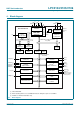
6. Functional description
6.1 Architectural overview
The ARM7TDMI-S is a general purpose 32-bit microprocessor, which offers high
performance and very low power consumption. The ARM architecture is based on
Reduced Instruction Set Computer (RISC) principles, and the instruction set and related
decode mechanism are much simpler than those of microprogrammed Complex
Instruction Set Computers. This simplicity results in a high instruction throughput and
impressive real-time interrupt response from a small and cost-effective processor core.
Pipeline techniques are employed so that all parts of the processing and memory systems
can operate continuously. Typically, while one instruction is being executed, its successor
is being decoded, and a third instruction is being fetched from memory.
The ARM7TDMI-S processor also employs a unique architectural strategy known as
Thumb, which makes it ideally suited to high-volume applications with memory
restrictions, or applications where code density is an issue.
The key idea behind Thumb is that of a super-reduced instruction set. Essentially, the
ARM7TDMI-S processor has two instruction sets:
• The standard 32-bit ARM set.
• A 16-bit Thumb set.
The Thumb set’s 16-bit instruction length allows it to approach twice the density of
standard ARM code while retaining most of the ARM’s performance advantage over a
traditional 16-bit processor using 16-bit registers. This is possible because Thumb code
operates on the same 32-bit register set as ARM code.
Thumb code is able to provide up to 65 % of the code size of ARM, and 160 % of the
performance of an equivalent ARM processor connected to a 16-bit memory system.
6.2 On-chip flash program memory
The LPC2104/2105/2106 incorporate a 128 kB flash memory system. This memory may
be used for both code and data storage. Programming of the flash memory may be
accomplished in several ways. It may be programmed In System via the serial port. The
application program may also erase and/or program the flash while the application is
running, allowing a great degree of flexibility for data storage field firmware upgrades, etc.
When on-chip bootloader is used, 120 kB of flash memory is available for user code.
The LPC2104/2105/2106 flash memory provides a minimum of 100000 erase/write cycles
and 20 years of data retention.
6.3 On-chip static RAM
On-chip static RAM may be used for code and/or data storage. The SRAM may be
accessed as 8 bit, 16 bit, and 32 bit. The LPC2104/2105/2106 provide 16/32/64 kB of
static RAM, respectively.