
Datasheet


LPC2104_2105_2106_7 © NXP B.V. 2008. All rights reserved.
Product data sheet Rev. 07 — 20 June 2008 7 of 41
NXP Semiconductors
LPC2104/2105/2106
Single-chip 32-bit microcontrollers
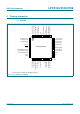
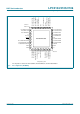
5.2 Pin description
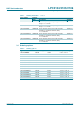
Table 3. Pin description
Symbol Pin Type Description
P0.0 to P0.31 I/O Port 0: Port 0 is a 32-bit bidirectional I/O port with individual direction controls for
each bit. The operation of port 0 pins depends upon the pin function selected via
the Pin Connect Block.
P0.0/TXD0/PWM1 13
[1]
I/O P0.0 — Port 0 bit 0.
O TXD0 — Transmitter output for UART 0.
O PWM1 — Pulse Width Modulator output 1.
P0.1/RXD0/PWM3 14
[1]
I/O P0.1 — Port 0 bit 1.
I RXD0 — Receiver input for UART 0.
O PWM3 — Pulse Width Modulator output 3.
P0.2/SCL/CAP0.0 18
[2]
I/O P0.2 — Port 0 bit 2. The output is open-drain.
I/O SCL — I
2
C-bus clock input/output. Open-drain output (for I
2
C-bus compliance).
I CAP0.0 — Capture input for Timer 0, channel 0.
P0.3/SDA/MAT0.0 21
[2]
I/O P0.3 — Port 0 bit 3. The output is open-drain.
I/O SDA — I
2
C-bus data input/output. Open-drain output (for I
2
C-bus compliance).
O MAT0.0 — Match output for Timer 0, channel 0. The output is open-drain.
P0.4/SCK/CAP0.1 22
[1]
I/O P0.4 — Port 0 bit 4.
I/O SCK — Serial clock for SPI/SSP
[3]
. Clock output from master or input to slave.
I CAP0.1 — Capture input for Timer 0, channel 1.
P0.5/MISO/MAT0.1 23
[1]
I/O P0.5 — Port 0 bit 5.
I/O MISO — Master In Slave Out for SPI/SSP
[3]
. Data input to SPI/SSP master or
data output from SPI/SSP slave.
O MAT0.1 — Match output for Timer 0, channel 1.
P0.6/MOSI/CAP0.2 24
[1]
I/O P0.6 — Port 0 bit 6.
I/O MOSI — Master Out Slave In for SPI/SSP
[3]
. Data output from SPI/SSP master
or data input to SPI/SSP slave.
I CAP0.2 — Capture input for Timer 0, channel 2.
P0.7/SSEL/PWM2 28
[1]
I/O P0.7 — Port 0 bit 7.
I SSEL — Slave Select for SPI/SSP
[3]
. Selects the SPI/SSP interface as a slave.
O PWM2 — Pulse Width Modulator output 2.
P0.8/TXD1/PWM4 29
[1]
I/O P0.8 — Port 0 bit 8.
O TXD1 — Transmitter output for UART 1.
O PWM4 — Pulse Width Modulator output 4.
P0.9/RXD1/PWM6 30
[1]
I/O P0.9 — Port 0 bit 9.
I RXD1 — Receiver input for UART 1.
O PWM6 — Pulse Width Modulator output 6.
P0.10/RTS1/CAP1.0 35
[1]
I/O P0.10 — Port 0 bit 10.
O RTS1 — Request to Send output for UART 1.
I CAP1.0 — Capture input for Timer 1, channel 0.