
Datasheet


LPC2104_2105_2106_7 © NXP B.V. 2008. All rights reserved.
Product data sheet Rev. 07 — 20 June 2008 9 of 41
NXP Semiconductors
LPC2104/2105/2106
Single-chip 32-bit microcontrollers
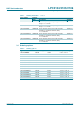
[1] 5 V tolerant pad providing digital I/O functions with TTL levels and hysteresis and 10 ns slew rate control.
[2] Open-drain 5 V tolerant digital I/O pad, compatible with I
2
C-bus 400 kHz specification. It requires external pull-up to provide an output
functionality. Open-drain configuration applies to all functions on this pin.
[3] SSP interface available on LPC2104/2105/2106/01 only.
[4] 5 V tolerant pad with built-in pull-up resistor providing digital I/O functions with TTL levels and hysteresis and 10 ns slew rate control.
The pull-up resistor’s value ranges from 60 kΩ to 300 kΩ.
[5] 5 V tolerant pad providing digital input (with TTL levels and hysteresis) function only.
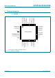
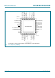
P0.26/TRACESYNC 39
[4]
I/O P0.26 — Port 0 bit 26.
O TRACESYNC — Trace Synchronization Standard I/O port with internal pull-up.
P0.27/TRACEPKT0/
TRST
8
[4]
I/O P0.27 — Port 0 bit 27.
O TRACEPKT0 — Trace Packet, bit 0. Standard I/O port with internal pull-up.
I TRST — Test Reset for JTAG interface, secondary JTAG pin group.
P0.28/TRACEPKT1/
TMS
9
[4]
I/O P0.28 — Port 0 bit 28.
O TRACEPKT1 — Trace Packet, bit 1. Standard I/O port with internal pull-up.
I TMS — Test Mode Select for JTAG interface, secondary JTAG pin group.
P0.29/TRACEPKT2/
TCK
10
[4]
I/O P0.29 — Port 0 bit 29.
O TRACEPKT2 — Trace Packet, bit 2. Standard I/O port with internal pull-up.
I TCK — Test Clock for JTAG interface, secondary JTAG pin group. This clock
must be slower than 1/6 of the CPU clock (CCLK) for the JTAG interface to
operate.
P0.30/TRACEPKT3/
TDI
15
[4]
I/O P0.30 — Port 0 bit 30.
O TRACEPKT3 — Trace Packet, bit 3. Standard I/O port with internal pull-up.
I TDI — Test Data In for JTAG interface, secondary JTAG pin group.
P0.31/EXTIN0/TDO 16
[4]
I/O P0.31 — Port 0 bit 31.
I EXTIN0 — External Trigger Input. Standard I/O port with internal pull-up.
O TDO — Test Data out for JTAG interface, secondary JTAG pin group.
RTCK 26
[4]
I/O Returned Test Clock output: Extra signal added to the JTAG port. Assists
debugger synchronization when processor frequency varies. Also used during
debug mode entry to select primary or secondary JTAG pins with the 48-pin
package. Bidirectional pin with internal pull-up.
DBGSEL 27 I Debug Select: When LOW, the part operates normally. When HIGH, debug
mode is entered. Input pin with internal pull-down.
RESET 6
[5]
I external reset input; a LOW on this pin resets the device, causing I/O ports and
peripherals to take on their default states, and processor execution to begin at
address 0. TTL with hysteresis, 5 V tolerant.
XTAL1 11 I input to the oscillator circuit and internal clock generator circuits.
XTAL2 12 O output from the oscillator amplifier.
V
SS
7, 19,
31, 43
I ground: 0 V reference.
V
DD(1V8)
5 I 1.8 V core power supply; this is the power supply voltage for internal circuitry.
V
DD(3V3)
17, 40 I 3.3 V pad power supply; this is the power supply voltage for the I/O ports.
n.c. 4, 20,
25, 42
- not connected; these pins are not connected in the 48-pin package.
Table 3. Pin description
…continued
Symbol Pin Type Description