LPC2377/78 Single-chip 16-bit/32-bit microcontrollers; 512 kB flash with ISP/IAP, Ethernet, USB 2.0, CAN, and 10-bit ADC/DAC Rev. 6.1 — 16 October 2013 Product data sheet 1. General description The LPC2377/78 microcontrollers are based on a 16-bit/32-bit ARM7TDMI-S CPU with real-time emulation that combines the microcontroller with 512 kB of embedded high-speed flash memory. A 128-bit wide memory interface and a unique accelerator architecture enable 32-bit code execution at the maximum clock rate.
LPC2377/78 NXP Semiconductors Single-chip 16-bit/32-bit microcontrollers General Purpose DMA controller (GPDMA) on AHB that can be used with the SSP serial interfaces, the I2S port, and the Secure Digital/MultiMediaCard (SD/MMC) card port, as well as for memory-to-memory transfers. Serial Interfaces: Ethernet MAC with associated DMA controller. These functions reside on an independent AHB. USB 2.0 full-speed device with on-chip PHY and associated DMA controller (LPC2378 only).
LPC2377/78 NXP Semiconductors Single-chip 16-bit/32-bit microcontrollers On-chip crystal oscillator with an operating range of 1 MHz to 25 MHz. 4 MHz internal RC oscillator trimmed to 1 % accuracy that can optionally be used as the system clock. When used as the CPU clock, does not allow CAN and USB to run. On-chip PLL allows CPU operation up to the maximum CPU rate without the need for a high frequency crystal. Can be run from the main oscillator, the internal RC oscillator, or the RTC oscillator.
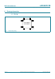
LPC2377/78 NXP Semiconductors Single-chip 16-bit/32-bit microcontrollers 5.
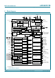
LPC2377/78 NXP Semiconductors Single-chip 16-bit/32-bit microcontrollers 6. Pinning information 109 144 6.1 Pinning 1 108 LPC2377FBD144 LPC2378FBD144 Fig 2. 72 73 37 36 002aac584 LPC2377/78 pinning LPC2377_78 Product data sheet All information provided in this document is subject to legal disclaimers. Rev. 6.1 — 16 October 2013 © NXP B.V. 2013. All rights reserved.
LPC2377/78 NXP Semiconductors Single-chip 16-bit/32-bit microcontrollers 6.2 Pin description Table 3.
LPC2377/78 NXP Semiconductors Single-chip 16-bit/32-bit microcontrollers Table 3. Pin description …continued Symbol Pin Type Description P0[9]/ I2STX_SDA/ MOSI1/MAT2[3] 109[1] I/O P0[9] — General purpose digital input/output pin. I/O I2STX_SDA — Transmit data. It is driven by the transmitter and read by the receiver. Corresponds to the signal SD in the I2S-bus specification. I/O MOSI1 — Master Out Slave In for SSP1. O MAT2[3] — Match output for Timer 2, channel 3.
LPC2377/78 NXP Semiconductors Single-chip 16-bit/32-bit microcontrollers Table 3. Pin description …continued Symbol Pin Type Description P0[18]/DCD1/ MOSI0/MOSI 86[1] I/O P0[18] — General purpose digital input/output pin. I DCD1 — Data Carrier Detect input for UART1. I/O MOSI0 — Master Out Slave In for SSP0. I/O MOSI — Master Out Slave In for SPI. I/O P0[19] — General purpose digital input/output pin. I DSR1 — Data Set Ready input for UART1.
LPC2377/78 NXP Semiconductors Single-chip 16-bit/32-bit microcontrollers Table 3. Pin description …continued Symbol Pin Type Description P0[28]/SCL0 34[4] I/O P0[28] — General purpose digital input/output pin. Output is open-drain. I/O SCL0 — I2C0 clock input/output. Open-drain output (for I2C-bus compliance). I/O P0[29] — General purpose digital input/output pin. I/O USB_D+1 — USB1 port bidirectional D+ line. (LPC2378 only) I/O P0[30] — General purpose digital input/output pin.
LPC2377/78 NXP Semiconductors Single-chip 16-bit/32-bit microcontrollers Table 3. Pin description …continued Symbol Pin Type Description P1[20]/PWM1[2]/ SCK0 49[1] I/O P1[20] — General purpose digital input/output pin. O PWM1[2] — Pulse Width Modulator 1, channel 2 output. I/O SCK0 — Serial clock for SSP0. P1[21]/PWM1[3]/ SSEL0 50[1] I/O P1[21] — General purpose digital input/output pin. O PWM1[3] — Pulse Width Modulator 1, channel 3 output. I/O SSEL0 — Slave Select for SSP0.
LPC2377/78 NXP Semiconductors Single-chip 16-bit/32-bit microcontrollers Table 3. Pin description …continued Symbol Pin Type Description P2[1]/PWM1[2]/ RXD1/ PIPESTAT0 106[1] I/O P2[1] — General purpose digital input/output pin. O PWM1[2] — Pulse Width Modulator 1, channel 2 output. I RXD1 — Receiver input for UART1. O PIPESTAT0 — Pipeline Status, bit 0. P2[2]/PWM1[3]/ CTS1/ PIPESTAT1 105[1] I/O P2[2] — General purpose digital input/output pin.
LPC2377/78 NXP Semiconductors Single-chip 16-bit/32-bit microcontrollers Table 3. Pin description …continued Symbol Pin Type Description P2[11]/EINT1/ MCIDAT1/ I2STX_CLK 75[6] I/O P2[11] — General purpose digital input/output pin. I EINT1 — External interrupt 1 input. O MCIDAT1 — Data line for SD/MMC interface. I/O I2STX_CLK — Transmit Clock. It is driven by the master and received by the slave. Corresponds to the signal SCK in the I2S-bus specification.
LPC2377/78 NXP Semiconductors Single-chip 16-bit/32-bit microcontrollers Table 3. Pin description …continued Symbol Pin Type Description P3[25]/MAT0[0]/ PWM1[2] 39[1] I/O P3[25] — General purpose digital input/output pin. O MAT0[0] — Match output for Timer 0, channel 0. O PWM1[2] — Pulse Width Modulator 1, output 2. P3[26]/MAT0[1]/ PWM1[3] 38[1] I/O P3[26] — General purpose digital input/output pin. O MAT0[1] — Match output for Timer 0, channel 1.
LPC2377/78 NXP Semiconductors Single-chip 16-bit/32-bit microcontrollers Table 3. Pin description …continued Symbol Pin Type Description P4[24]/OE 127[1] I/O P4[24] — General purpose digital input/output pin. O OE — LOW active Output Enable signal. P4[25]/BLS0 124[1] I/O P4[25] — General purpose digital input/output pin. O BLS0 — LOW active Byte Lane select signal 0. P4[28]/MAT2[0]/ TXD3 118[1] I/O P4[28] — General purpose digital input/output pin.
LPC2377/78 NXP Semiconductors Single-chip 16-bit/32-bit microcontrollers Table 3. Pin description …continued Symbol Pin VDD(3V3) 41, 62, I 77, 102, 114, 138[15] Type Description 3.3 V supply voltage: These pins provide power supply voltage for the I/O ports. n.c. 21, 81, 98[16] I Leave these pins unconnected. VDD(DCDC)(3V3) 18, 60, 121[17] I 3.3 V DC-to-DC converter supply voltage: These pins provide the power supply voltage for the on-chip DC-to-DC converter only.
LPC2377/78 NXP Semiconductors Single-chip 16-bit/32-bit microcontrollers 7. Functional description 7.1 Architectural overview The LPC2377/78 microcontrollers consist of an ARM7TDMI-S CPU with emulation support, the ARM7 local bus for closely coupled, high-speed access to most on-chip memory, the AMBA AHB interfacing to high-speed on-chip peripherals and external memory, and the AMBA APB for connection to other on-chip peripheral functions.
LPC2377/78 NXP Semiconductors Single-chip 16-bit/32-bit microcontrollers The 16-bit instruction length of the Thumb set allows it to approach twice the density of standard ARM code, while retaining most of the ARM performance advantage over a traditional 16-bit processor using 16-bit registers. This increase is possible because Thumb code operates on the same 32-bit register set as ARM code.
LPC2377/78 NXP Semiconductors Single-chip 16-bit/32-bit microcontrollers 7.4 Memory map The LPC2377/78 memory map incorporates several distinct regions as shown in Figure 3. In addition, the CPU interrupt vectors may be remapped to allow them to reside in either flash memory (default), boot ROM, or SRAM (see Section 7.26.6). 0xFFFF FFFF 4.0 GB AHB PERIPHERALS 0xF000 0000 3.75 GB APB PERIPHERALS 3.5 GB 0xE000 0000 RESERVED ADDRESS SPACE 3.
LPC2377/78 NXP Semiconductors Single-chip 16-bit/32-bit microcontrollers 7.5 Interrupt controller The ARM processor core has two interrupt inputs called Interrupt Request (IRQ) and Fast Interrupt Request (FIQ). The VIC takes 32 interrupt request inputs which can be programmed as FIQ or vectored IRQ types. The programmable assignment scheme means that priorities of interrupts from the various peripherals can be dynamically assigned and adjusted. FIQs have the highest priority.
LPC2377/78 NXP Semiconductors Single-chip 16-bit/32-bit microcontrollers 7.7.
LPC2377/78 NXP Semiconductors Single-chip 16-bit/32-bit microcontrollers • 32-bit AHB master bus width. • Incrementing or non-incrementing addressing for source and destination. • Programmable DMA burst size. The DMA burst size can be programmed to more efficiently transfer data. Usually the burst size is set to half the size of the FIFO in the peripheral. • Internal four-word FIFO per channel. • Supports 8-bit, 16-bit, and 32-bit wide transactions.
LPC2377/78 NXP Semiconductors Single-chip 16-bit/32-bit microcontrollers 7.10 Ethernet The Ethernet block contain a full featured 10 Mbit/s or 100 Mbit/s Ethernet MAC designed to provide optimized performance through the use of DMA hardware acceleration. Features include a generous suite of control registers, half or full duplex operation, flow control, control frames, hardware acceleration for transmit retry, receive packet filtering and wake-up on LAN activity.
LPC2377/78 NXP Semiconductors Single-chip 16-bit/32-bit microcontrollers • Physical interface: – Attachment of external PHY chip through standard RMII interface. – PHY register access is available via the MIIM interface. 7.11 USB interface (LPC2378 only) The Universal Serial Bus (USB) is a 4-wire bus that supports communication between a host and a number (127 maximum) of peripherals. The host controller allocates the USB bandwidth to attached devices through a token based protocol.
LPC2377/78 NXP Semiconductors Single-chip 16-bit/32-bit microcontrollers 7.12 CAN controller and acceptance filters (LPC2378 only) The Controller Area Network (CAN) is a serial communications protocol which efficiently supports distributed real-time control with a very high level of security. Its domain of application ranges from high-speed networks to low cost multiplex wiring.
LPC2377/78 NXP Semiconductors Single-chip 16-bit/32-bit microcontrollers 7.14 10-bit DAC The DAC allows the LPC2377/78 to generate a variable analog output. The maximum output value of the DAC is Vi(VREF). 7.14.1 Features • • • • • 10-bit DAC Resistor string architecture Buffered output Power-down mode Selectable output drive 7.15 UARTs The LPC2377/78 contain four UARTs. In addition to standard transmit and receive data lines, UART1 also provides a full modem control handshake interface.
LPC2377/78 NXP Semiconductors Single-chip 16-bit/32-bit microcontrollers 7.17 SSP serial I/O controller The LPC2377/78 contain two SSP controllers. The SSP controller is capable of operation on a SPI, 4-wire SSI, or Microwire bus. It can interact with multiple masters and slaves on the bus. Only a single master and a single slave can communicate on the bus during a given data transfer.
LPC2377/78 NXP Semiconductors Single-chip 16-bit/32-bit microcontrollers 7.19.1 Features • I2C0 is a standard I2C compliant bus interface with open-drain pins. • I2C1 and I2C2 use standard I/O pins and do not support powering off of individual devices connected to the same bus lines. • • • • • Easy to configure as master, slave, or master/slave. Programmable clocks allow versatile rate control. Bidirectional data transfer between masters and slaves. Multi-master bus (no central master).
LPC2377/78 NXP Semiconductors Single-chip 16-bit/32-bit microcontrollers 7.21 General purpose 32-bit timers/external event counters The LPC2377/78 include four 32-bit Timer/Counters. The Timer/Counter is designed to count cycles of the system derived clock or an externally-supplied clock. It can optionally generate interrupts or perform other actions at specified timer values, based on four match registers.
LPC2377/78 NXP Semiconductors Single-chip 16-bit/32-bit microcontrollers Three match registers can be used to provide a PWM output with both edges controlled. Again, the PWMMR0 match register controls the PWM cycle rate. The other match registers control the two PWM edge positions. Additional double edge controlled PWM outputs require only two match registers each, since the repetition rate is the same for all PWM outputs.
LPC2377/78 NXP Semiconductors Single-chip 16-bit/32-bit microcontrollers 7.23 Watchdog timer The purpose of the watchdog is to reset the microcontroller within a reasonable amount of time if it enters an erroneous state. When enabled, the watchdog will generate a system reset if the user program fails to ‘feed’ (or reload) the watchdog within a predetermined amount of time. 7.23.1 Features • Internally resets chip if not periodically reloaded. • Debug mode.
LPC2377/78 NXP Semiconductors Single-chip 16-bit/32-bit microcontrollers 7.24 RTC and battery RAM The RTC is a set of counters for measuring time when system power is on, and optionally when it is off. It uses little power in Power-down and Deep power-down modes. On the LPC2377/78, the RTC can be clocked by a separate 32.768 kHz oscillator or by a programmable prescale divider based on the APB clock.
LPC2377/78 NXP Semiconductors Single-chip 16-bit/32-bit microcontrollers 7.25.1.2 Main oscillator The main oscillator can be used as the clock source for the CPU, with or without using the PLL. The main oscillator operates at frequencies of 1 MHz to 25 MHz. This frequency can be boosted to a higher frequency, up to the maximum CPU operating frequency, by the PLL. The clock selected as the PLL input is PLLCLKIN. The ARM processor clock frequency is referred to as CCLK elsewhere in this document.
LPC2377/78 NXP Semiconductors Single-chip 16-bit/32-bit microcontrollers amplitude to drive the clock logic. The amount of time depends on many factors, including the rate of VDD(3V3) ramp (in the case of power-on), the type of crystal and its electrical characteristics (if a quartz crystal is used), as well as any other external circuitry (e.g., capacitors), and the characteristics of the oscillator itself under the existing ambient conditions. 7.25.
LPC2377/78 NXP Semiconductors Single-chip 16-bit/32-bit microcontrollers 7.25.4.3 Power-down mode Power-down mode does everything that Sleep mode does, but also turns off the IRC oscillator and the flash memory. This saves more power, but requires waiting for resumption of flash operation before execution of code or data access in the flash memory can be accomplished. On the wake-up of Power-down mode, if the IRC was used before entering Power-down mode, it will take IRC 60 s to start-up.
LPC2377/78 NXP Semiconductors Single-chip 16-bit/32-bit microcontrollers The VBAT pin supplies power only to the RTC and the battery RAM. These two functions require a minimum of power to operate, which can be supplied by an external battery. When the CPU and the rest of chip functions are stopped and power removed, the RTC can supply an alarm output that may be used by external hardware to restore chip power and resume operation. 7.26 System control 7.26.
LPC2377/78 NXP Semiconductors Single-chip 16-bit/32-bit microcontrollers Running an application with level CRP3 selected fully disables any access to chip via the JTAG pins and the ISP. This mode effectively disables ISP override using P2[10] pin, too. It is up to the user’s application to provide (if needed) flash update mechanism using IAP calls or call reinvoke ISP command to enable flash update via UART0.
LPC2377/78 NXP Semiconductors Single-chip 16-bit/32-bit microcontrollers 7.27.1 EmbeddedICE The EmbeddedICE logic provides on-chip debug support. The debugging of the target system requires a host computer running the debugger software and an EmbeddedICE protocol convertor. The EmbeddedICE protocol convertor converts the Remote Debug Protocol commands to the JTAG data needed to access the ARM7TDMI-S core present on the target system. The ARM core has a Debug Communication Channel (DCC) function built-in.
LPC2377/78 NXP Semiconductors Single-chip 16-bit/32-bit microcontrollers 8. Limiting values Table 4. Limiting values In accordance with the Absolute Maximum Rating System (IEC 60134).[1] Symbol Parameter Conditions Min Max Unit VDD(3V3) supply voltage (3.3 V) core and external rail 3.0 3.6 V 3.0 3.6 V 0.5 +4.6 V 0.5 +4.6 V 0.5 +4.6 V 0.5 +5.1 V [2] 0.5 +6.0 V other I/O pins [2][3] 0.5 VDD(3V3) + 0.
LPC2377/78 NXP Semiconductors Single-chip 16-bit/32-bit microcontrollers 9. Thermal characteristics The average chip junction temperature, Tj (C), can be calculated using the following equation: T j = T amb + P D R th j – a (1) • Tamb = ambient temperature (C) • Rth(j-a) = the package junction-to-ambient thermal resistance (C/W) • PD = sum of internal and I/O power dissipation The internal power dissipation is the product of IDD and VDD.
LPC2377/78 NXP Semiconductors Single-chip 16-bit/32-bit microcontrollers 10. Static characteristics Table 7. Static characteristics Tamb = 40 C to +85 C for commercial applications, unless otherwise specified. Symbol Parameter Conditions Min Typ[1] Max Unit VDD(3V3) supply voltage (3.3 V) core and external rail 3.0 3.3 3.6 V VDD(DCDC)(3V3) DC-to-DC converter supply voltage (3.3 V) 3.0 3.3 3.6 V VDDA analog 3.3 V pad supply voltage 3.0 3.3 3.
LPC2377/78 NXP Semiconductors Single-chip 16-bit/32-bit microcontrollers Table 7. Static characteristics …continued Tamb = 40 C to +85 C for commercial applications, unless otherwise specified. Symbol Parameter Conditions Min Typ[1] Max Unit Ilatch I/O latch-up current (0.5VDD(3V3)) < VI < (1.5VDD(3V3)); - - 100 mA 0 - 5.
LPC2377/78 NXP Semiconductors Single-chip 16-bit/32-bit microcontrollers Table 7. Static characteristics …continued Tamb = 40 C to +85 C for commercial applications, unless otherwise specified. Symbol Parameter Vo(RTCX2) output voltage on pin RTCX2 Conditions Min Typ[1] Max Unit 0.5 1.8 1.95 V - - 10 A - - 5.25 V USB pins (LPC2378 only) IOZ OFF-state output current 0 V < VI < 3.3 V VBUS bus supply voltage VDI differential input sensitivity voltage (D+) (D) 0.
LPC2377/78 NXP Semiconductors Single-chip 16-bit/32-bit microcontrollers 10.1 Power-down mode 002aae049 4 IDD(IO) (μA) 2 VDD(3V3) = 3.3 V VDD(3V3) = 3.0 V 0 −2 −4 −40 −15 10 35 60 85 temperature (°C) Vi(VBAT) = VDD(DCDC)(3V3) = 3.3 V; Tamb = 25 C. Fig 4. I/O maximum supply current IDD(IO) versus temperature in Power-down mode 002aae050 40 IBAT (μA) 30 Vi(VBAT) = 3.3 V Vi(VBAT) = 3.0 V 20 10 0 −40 −15 10 35 60 85 temperature (°C) VDD(3V3) = VDD(DCDC)(3V3) = 3.3 V; Tamb = 25 C. Fig 5.
LPC2377/78 NXP Semiconductors Single-chip 16-bit/32-bit microcontrollers 002aae051 800 IDD(DCDC)pd(3v3) (μA) 600 400 VDD(DCDC)(3V3) = 3.3 V 200 0 −40 VDD(DCDC)(3V3) = 3.0 V −15 10 35 60 85 temperature (°C) VDD(3V3) = Vi(VBAT) = 3.3 V; Tamb = 25 C. Fig 6. Total DC-to-DC converter supply current IDD(DCDC)pd(3V3) at different temperatures in Power-down mode 10.2 Deep power-down mode 002aae046 300 IDD(IO) (μA) 200 100 VDD(3V3) = 3.3 V VDD(3V3) = 3.
LPC2377/78 NXP Semiconductors Single-chip 16-bit/32-bit microcontrollers 002aae047 40 IBAT (μA) 30 Vi(VBAT) = 3.3 V Vi(VBAT) = 3.0 V 20 10 0 −40 −15 10 35 60 85 temperature (°C) VDD(3V3) = VDD(DCDC)(3V3) = 3.3 V; Tamb = 25 C Fig 8. RTC battery maximum supply current IBAT versus temperature in Deep power-down mode 002aae048 100 IDD(DCDC)dpd(3v3) (μA) 80 60 VDD(DCDC)(3V3) = 3.3 V 40 VDD(DCDC)(3V3) = 3.0 V 20 0 −40 −15 10 35 60 85 temperature (°C) VDD(3V3) = Vi(VBAT) = 3.
LPC2377/78 NXP Semiconductors Single-chip 16-bit/32-bit microcontrollers 10.3 Electrical pin characteristics 002aaf112 3.6 VOH (V) T = 85 °C 25 °C −40 °C 3.2 2.8 2.4 2.0 0 8 16 24 IOH (mA) Conditions: VDD(3V3) = 3.3 V; standard port pins. Fig 10. Typical HIGH-level output voltage VOH versus HIGH-level output source current IOH 002aaf111 15 IOL (mA) T = 85 °C 25 °C −40 °C 10 5 0 0 0.2 0.4 0.6 VOL (V) Conditions: VDD(3V3) = 3.3 V; standard port pins. Fig 11.
LPC2377/78 NXP Semiconductors Single-chip 16-bit/32-bit microcontrollers 11. Dynamic characteristics Table 8. Dynamic characteristics Tamb = 40 C to +85 C for commercial applications; VDD(3V3) over specified ranges.[1] Symbol Parameter Conditions Typ[2] Min Max Unit External clock (see Figure 12) fosc oscillator frequency 1 - 25 MHz Tcy(clk) clock cycle time 40 - 1000 ns tCHCX clock HIGH time Tcy(clk) 0.4 - - ns tCLCX clock LOW time Tcy(clk) 0.
LPC2377/78 NXP Semiconductors Single-chip 16-bit/32-bit microcontrollers 11.1 Internal oscillators Table 9. Dynamic characteristic: internal oscillators Tamb = 40 C to +85 C; 3.0 V VDD(3V3) 3.6 V.[1] Symbol Parameter Conditions Min Typ[2] Max Unit fosc(RC) internal RC oscillator frequency - 3.96 4.02 4.04 MHz fi(RTC) RTC input frequency - - 32.768 - kHz Max Unit [1] Parameters are valid over operating temperature range unless otherwise specified.
LPC2377/78 NXP Semiconductors Single-chip 16-bit/32-bit microcontrollers 11.4 Flash memory Table 12. Dynamic characteristics of flash Tamb = 40 C to +85 C, unless otherwise specified; VDD(3V3) = 3.0 V to 3.6 V; all voltages are measured with respect to ground.
xxxxxxxxxxxxxxxxxxxxx xxxxxxxxxxxxxxxxxxxxxxxxxx xxxxxxx x x x xxxxxxxxxxxxxxxxxxxxxxxxxxxxxx xxxxxxxxxxxxxxxxxxx xx xx xxxxx xxxxxxxxxxxxxxxxxxxxxxxxxxx xxxxxxxxxxxxxxxxxxx xxxxxx xxxxxxxxxxxxxxxxxxxxxxxxxxxxxxxxxxx xxxxxxxxxxxx x x xxxxxxxxxxxxxxxxxxxxx xxxxxxxxxxxxxxxxxxxxxxxxxxxxxx xxxxx xxxxxxxxxxxxxxxxxxxxxxxxxxxxxxxxxxxxxxxxxxxxxxxxxx xxxxxxxx xxxxxxxxxxxxxxxxxxxxxxxxx xxxxxxxxxxxxxxxxxxxx xxx NXP Semiconductors LPC2377_78 Product data sheet 11.5 Static external memory interface Table 13.
LPC2377/78 NXP Semiconductors Single-chip 16-bit/32-bit microcontrollers 11.6 Timing tCSLAV tCSHOEH CS addr tam th(D) data tCSLOEL tOELAV tOEHANV tOELOEH OE 002aaf489 Fig 13. External memory read access CS tCSLAV tBLSLBLSH BLS tCSLBLSL tBLSDV tBLSHANV addr tCSLDV tBLSHDNV data OE 002aaf490 Fig 14. External memory write access LPC2377_78 Product data sheet All information provided in this document is subject to legal disclaimers. Rev. 6.1 — 16 October 2013 © NXP B.V. 2013.
LPC2377/78 NXP Semiconductors Single-chip 16-bit/32-bit microcontrollers TPERIOD crossover point extended crossover point differential data lines source EOP width: tFEOPT differential data to SE0/EOP skew n × TPERIOD + tFDEOP receiver EOP width: tEOPR1, tEOPR2 002aab561 Fig 15. Differential data-to-EOP transition skew and EOP width shifting edges SCK sampling edges MOSI MISO tsu(SPI_MISO) 002aad326 Fig 16.
LPC2377/78 NXP Semiconductors Single-chip 16-bit/32-bit microcontrollers 12. ADC electrical characteristics Table 14. ADC electrical characteristics VDDA = 2.5 V to 3.6 V; Tamb = 40 C to +85 C unless otherwise specified; ADC frequency 4.5 MHz.
LPC2377/78 NXP Semiconductors Single-chip 16-bit/32-bit microcontrollers offset error EO gain error EG 1023 1022 1021 1020 1019 1018 (2) 7 code out (1) 6 5 (5) 4 (4) 3 (3) 2 1 LSB (ideal) 1 0 1 2 3 4 5 6 7 1018 1019 1020 1021 1022 1023 1024 VIA (LSBideal) offset error EO 1 LSB = Vi(VREF) − VSSA 1024 002aae604 (1) Example of an actual transfer curve. (2) The ideal transfer curve. (3) Differential linearity error (ED). (4) Integral non-linearity (EL(adj)).
LPC2377/78 NXP Semiconductors Single-chip 16-bit/32-bit microcontrollers LPC23XX 20 kΩ AD0[y] AD0[y]SAMPLE 3 pF Rvsi 5 pF VEXT VSS 002aac610 Fig 18. Suggested ADC interface - LPC2377/78 AD0[y] pin LPC2377_78 Product data sheet All information provided in this document is subject to legal disclaimers. Rev. 6.1 — 16 October 2013 © NXP B.V. 2013. All rights reserved.
LPC2377/78 NXP Semiconductors Single-chip 16-bit/32-bit microcontrollers 13. DAC electrical characteristics Table 15. DAC electrical characteristics VDDA = 3.0 V to 3.6 V; Tamb = 40 C to +85 C unless otherwise specified Symbol Parameter ED Conditions Min Typ Max Unit differential linearity error - 1 - LSB EL(adj) integral non-linearity - 1.5 - LSB EO offset error - 0.6 - % EG gain error - 0.
LPC2377/78 NXP Semiconductors Single-chip 16-bit/32-bit microcontrollers VDD(3V3) R2 LPC23XX USB_UP_LED R1 1.5 kΩ VBUS USB_D+ RS = 33 Ω USB-B connector USB_D− RS = 33 Ω VSS 002aac579 Fig 20. LPC2378 USB interface on a bus-powered device 14.2 Crystal oscillator XTAL input and component selection The input voltage to the on-chip oscillators is limited to 1.8 V. If the oscillator is driven by a clock in slave mode, it is recommended that the input be coupled through a capacitor with Ci = 100 pF.
LPC2377/78 NXP Semiconductors Single-chip 16-bit/32-bit microcontrollers LPC2xxx L XTALIN XTALOUT = CL CP XTAL RS CX2 CX1 002aaf494 Fig 22. Oscillator modes and models: oscillation mode of operation and external crystal model used for CX1/CX2 evaluation Table 16.
LPC2377/78 NXP Semiconductors Single-chip 16-bit/32-bit microcontrollers 14.3 RTC 32 kHz oscillator component selection LPC2xxx L RTCX1 RTCX2 = CL CP 32 kHz XTAL RS CX1 CX2 002aaf495 Fig 23. RTC oscillator modes and models: oscillation mode of operation and external crystal model used for CX1/CX2 evaluation The RTC external oscillator circuit is shown in Figure 23.
LPC2377/78 NXP Semiconductors Single-chip 16-bit/32-bit microcontrollers 14.5 Standard I/O pin configuration Figure 24 shows the possible pin modes for standard I/O pins with analog input function: • • • • Digital output driver Digital input: Pull-up enabled/disabled Digital input: Pull-down enabled/disabled Analog input (for ADC input channels) The default configuration for standard I/O pins is input with pull-up enabled.
LPC2377/78 NXP Semiconductors Single-chip 16-bit/32-bit microcontrollers 14.6 Reset pin configuration VDD VDD VDD Rpu reset ESD 20 ns RC GLITCH FILTER PIN ESD VSS 002aaf274 Fig 25. Reset pin configuration LPC2377_78 Product data sheet All information provided in this document is subject to legal disclaimers. Rev. 6.1 — 16 October 2013 © NXP B.V. 2013. All rights reserved.
LPC2377/78 NXP Semiconductors Single-chip 16-bit/32-bit microcontrollers 15. Package outline LQFP144: plastic low profile quad flat package; 144 leads; body 20 x 20 x 1.4 mm SOT486-1 c y X A 73 72 108 109 ZE e E HE A A2 (A 3) A1 θ wM Lp bp L pin 1 index detail X 37 144 1 36 v M A ZD wM bp e D B HD v M B 0 5 10 mm scale DIMENSIONS (mm are the original dimensions) UNIT A max. A1 A2 A3 bp c D (1) E (1) e mm 1.6 0.15 0.05 1.45 1.35 0.25 0.27 0.17 0.20 0.09 20.
LPC2377/78 NXP Semiconductors Single-chip 16-bit/32-bit microcontrollers 16. Abbreviations Table 19.
LPC2377/78 NXP Semiconductors Single-chip 16-bit/32-bit microcontrollers 17. Revision history Table 20. Revision history Document ID Release date Data sheet status Change notice Supersedes LPC2377_78 v.6.1 20131016 Product data sheet - LPC2377_78 v.6 Modifications: LPC2377_78 v.6 Modifications: • • Table 3 “Pin description”, Table note 6: Changed glitch filter spec from 5 ns to 10 ns. Table 8 “Dynamic characteristics”: Changed min clock cycle time from 42 to 40.
LPC2377/78 NXP Semiconductors Single-chip 16-bit/32-bit microcontrollers Table 20. Revision history …continued Document ID Release date Data sheet status Change notice Supersedes LPC2377_78 v.5 20100617 Product data sheet - LPC2377_78 v.4 Modifications: • • • • • • • Table 3 “Pin description”: Added Table note 9 for XTAL1 and XTAL2 pins. Table 3 “Pin description”: Added Table note 10 for RTCX1 and RTCX2 pins. Table 4 “Limiting values”: Changed VESD min/max to 2500/+2500.
LPC2377/78 NXP Semiconductors Single-chip 16-bit/32-bit microcontrollers 18. Legal information 18.1 Data sheet status Document status[1][2] Product status[3] Definition Objective [short] data sheet Development This document contains data from the objective specification for product development. Preliminary [short] data sheet Qualification This document contains data from the preliminary specification. Product [short] data sheet Production This document contains the product specification.
LPC2377/78 NXP Semiconductors Single-chip 16-bit/32-bit microcontrollers Export control — This document as well as the item(s) described herein may be subject to export control regulations. Export might require a prior authorization from competent authorities. Non-automotive qualified products — Unless this data sheet expressly states that this specific NXP Semiconductors product is automotive qualified, the product is not suitable for automotive use.
LPC2377/78 NXP Semiconductors Single-chip 16-bit/32-bit microcontrollers 20. Contents 1 General description . . . . . . . . . . . . . . . . . . . . . . 1 2 Features and benefits . . . . . . . . . . . . . . . . . . . . 1 3 Applications . . . . . . . . . . . . . . . . . . . . . . . . . . . . 3 4 Ordering information . . . . . . . . . . . . . . . . . . . . . 3 4.1 Ordering options . . . . . . . . . . . . . . . . . . . . . . . . 3 5 Block diagram . . . . . . . . . . . . . . . . . . . . . . . . . .
LPC2377/78 NXP Semiconductors Single-chip 16-bit/32-bit microcontrollers 12 13 14 14.1 14.2 14.3 14.4 14.5 14.6 15 16 17 18 18.1 18.2 18.3 18.4 19 20 ADC electrical characteristics . . . . . . . . . . . . DAC electrical characteristics . . . . . . . . . . . . Application information. . . . . . . . . . . . . . . . . . Suggested USB interface solutions (LPC2378 only). . . . . . . . . . . . . . . . . . . . . . . . Crystal oscillator XTAL input and component selection . . . . . . . . . . . . . . . . . . . .