
Datasheet

LPC2377_78 All information provided in this document is subject to legal disclaimers. © NXP B.V. 2013. All rights reserved.
Product data sheet Rev. 6.1 — 16 October 2013 6 of 69
NXP Semiconductors
LPC2377/78
Single-chip 16-bit/32-bit microcontrollers
6.2 Pin description
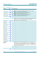
Table 3. Pin description
Symbol Pin Type Description
P0[0] to P0[31] I/O Port 0: Port 0 is a 32-bit I/O port with individual direction controls for each bit. The
operation of port 0 pins depends upon the pin function selected via the pin connect
block.
P0[0]/RD1/TXD/
SDA1
66
[1]
I/O P0[0] — General purpose digital input/output pin.
I RD1 — CAN1 receiver input. (LPC2378 only)
O TXD3 — Transmitter output for UART3.
I/O SDA1 — I
2
C1 data input/output (this pin is not open-drain).
P0[1]/TD1/RXD3/
SCL1
67
[1]
I/O P0[1] — General purpose digital input/output pin.
O TD1 — CAN1 transmitter output. (LPC2378 only)
I RXD3 — Receiver input for UART3.
I/O SCL1 — I
2
C1 clock input/output (this pin is not open-drain).
P0[2]/TXD0 141
[1]
I/O P0[2] — General purpose digital input/output pin.
O TXD0 — Transmitter output for UART0.
P0[3]/RXD0 142
[1]
I/O P0[3] — General purpose digital input/output pin.
I RXD0 — Receiver input for UART0.
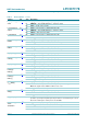
P0[4]/
I2SRX_CLK/
RD2/CAP2[0]
116
[1]
I/O P0[4] — General purpose digital input/output pin.
I/O I2SRX_CLK — Receive Clock. It is driven by the master and received by the slave.
Corresponds to the signal SCK in the I
2
S-bus specification.
I RD2 — CAN2 receiver input. (LPC2378 only)
I CAP2[0] — Capture input for Timer 2, channel 0.
P0[5]/
I2SRX_WS/
TD2/CAP2[1]
115
[1]
I/O P0[5] — General purpose digital input/output pin.
I/O I2SRX_WS — Receive Word Select. It is driven by the master and received by the
slave. Corresponds to the signal WS in the I
2
S-bus specification.
O TD2 — CAN2 transmitter output. (LPC2378 only)
I CAP2[1] — Capture input for Timer 2, channel 1.
P0[6]/
I2SRX_SDA/
SSEL1/MAT2[0]
113
[1]
I/O P0[6] — General purpose digital input/output pin.
I/O I2SRX_SDA — Receive data. It is driven by the transmitter and read by the
receiver. Corresponds to the signal SD in the I
2
S-bus specification.
I/O SSEL1 — Slave Select for SSP1.
O MAT2[0] — Match output for Timer 2, channel 0.
P0[7]/
I2STX_CLK/
SCK1/MAT2[1]
112
[1]
I/O P0[7] — General purpose digital input/output pin.
I/O I2STX_CLK — Transmit Clock. It is driven by the master and received by the slave.
Corresponds to the signal SCK in the I
2
S-bus specification.
I/O SCK1 — Serial Clock for SSP1.
O MAT2[1] — Match output for Timer 2, channel 1.
P0[8]/
I2STX_WS/
MISO1/MAT2[2]
111
[1]
I/O P0[8] — General purpose digital input/output pin.
I/O I2STX_WS — Transmit Word Select. It is driven by the master and received by the
slave. Corresponds to the signal WS in the I
2
S-bus specification.
I/O MISO1 — Master In Slave Out for SSP1.
O MAT2[2] — Match output for Timer 2, channel 2.