LPC2387 Single-chip 16-bit/32-bit MCU; 512 kB flash with ISP/IAP, Ethernet, USB 2.0 device/host/OTG, CAN, and 10-bit ADC/DAC Rev. 5.1 — 16 October 2013 Product data sheet 1. General description The LPC2387 microcontroller is based on a 16-bit/32-bit ARM7TDMI-S CPU with real-time emulation that combines the microcontroller with 512 kB of embedded high-speed flash memory. A 128-bit wide memory interface and a unique accelerator architecture enable 32-bit code execution at the maximum clock rate.
LPC2387 NXP Semiconductors Single-chip 16-bit/32-bit MCU Serial interfaces: Ethernet MAC with associated DMA controller. These functions reside on an independent AHB. USB 2.0 device/host/OTG with on-chip PHY and associated DMA controller. Four UARTs with fractional baud rate generation, one with modem control I/O, one with IrDA support, all with FIFO. CAN controller with two channels. SPI controller. Two SSP controllers, with FIFO and multi-protocol capabilities.
LPC2387 NXP Semiconductors Single-chip 16-bit/32-bit MCU On-chip PLL allows CPU operation up to the maximum CPU rate without the need for a high frequency crystal. May be run from the main oscillator, the internal RC oscillator, or the RTC oscillator. Versatile pin function selections allow more possibilities for using on-chip peripheral functions. 3. Applications Industrial control Medical systems Protocol converter Communications 4. Ordering information Table 1.
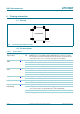
LPC2387 NXP Semiconductors Single-chip 16-bit/32-bit MCU 5.
LPC2387 NXP Semiconductors Single-chip 16-bit/32-bit MCU 6. Pinning information 76 100 6.1 Pinning 1 75 LPC2387FBD100 Fig 2. 50 51 26 25 002aad329 LPC2387 pinning LQFP100 package 6.2 Pin description Table 3.
LPC2387 NXP Semiconductors Single-chip 16-bit/32-bit MCU Table 3. Pin description …continued Symbol Pin Type Description P0[5]/I2SRX_WS/ TD2/CAP2[1] 80[1] I/O P0[5] — General purpose digital input/output pin. I/O I2SRX_WS — Receive Word Select. It is driven by the master and received by the slave. Corresponds to the signal WS in the I2S-bus specification. O TD2 — CAN2 transmitter output. I CAP2[1] — Capture input for Timer 2, channel 1.
LPC2387 NXP Semiconductors Single-chip 16-bit/32-bit MCU Table 3. Pin description …continued Symbol Pin Type Description P0[17]/CTS1/ MISO0/MISO 61[1] I/O P0[17] — General purpose digital input/output pin. I CTS1 — Clear to Send input for UART1. I/O MISO0 — Master In Slave Out for SSP0. I/O MISO — Master In Slave Out for SPI. I/O P0[18] — General purpose digital input/output pin. I DCD1 — Data Carrier Detect input for UART1. I/O MOSI0 — Master Out Slave In for SSP0.
LPC2387 NXP Semiconductors Single-chip 16-bit/32-bit MCU Table 3. Pin description …continued Symbol Pin Type Description P0[26]/AD0[3]/ AOUT/RXD3 6[3] I/O P0[26] — General purpose digital input/output pin. I AD0[3] — A/D converter 0, input 3. O AOUT — D/A converter output. I RXD3 — Receiver input for UART3. I/O P0[27] — General purpose digital input/output pin. I/O SDA0 — I2C0 data input/output. Open-drain output (for I2C-bus compliance).
LPC2387 NXP Semiconductors Single-chip 16-bit/32-bit MCU Table 3. Pin description …continued Symbol Pin Type Description P1[18]/ USB_UP_LED/ PWM1[1]/ CAP1[0] 32[1] I/O P1[18] — General purpose digital input/output pin. O USB_UP_LED — USB GoodLink LED indicator. It is LOW when device is configured (non-control endpoints enabled), or when host is enabled and has detected a device on the bus.
LPC2387 NXP Semiconductors Single-chip 16-bit/32-bit MCU Table 3. Pin description …continued Symbol Pin Type Description P1[27]/ USB_INT1/ USB_OVRCR1/ CAP0[1] 43[1] I/O P1[27] — General purpose digital input/output pin. I USB_INT1 — USB port 1 OTG transceiver interrupt (OTG transceiver). I USB_OVRCR1 — USB port 1 Over-Current status.
LPC2387 NXP Semiconductors Single-chip 16-bit/32-bit MCU Table 3. Pin description …continued Symbol Pin P2[4]/PWM1[5]/ 69[1] DSR1/TRACESYNC P2[5]/PWM1[6]/ DTR1/TRACEPKT0 68[1] P2[6]/PCAP1[0]/RI1/ 67[1] TRACEPKT1 P2[7]/RD2/ RTS1/TRACEPKT2 P2[8]/TD2/ TXD2/TRACEPKT3 P2[9]/ USB_CONNECT/ RXD2/EXTIN0 P2[10]/EINT0 66[1] 65[1] 64[1] 53[6] Type Description I/O P2[4] — General purpose digital input/output pin. O PWM1[5] — Pulse Width Modulator 1, channel 5 output.
LPC2387 NXP Semiconductors Single-chip 16-bit/32-bit MCU Table 3. Pin description …continued Symbol Pin Type Description P2[13]/EINT3/ MCIDAT3/ I2STX_SDA 50[6] I/O P2[13] — General purpose digital input/output pin. I EINT3 — External interrupt 3 input. O MCIDAT3 — Data line for SD/MMC interface. I/O I2STX_SDA — Transmit data. It is driven by the transmitter and read by the receiver. Corresponds to the signal SD in the I2S-bus specification.
LPC2387 NXP Semiconductors Single-chip 16-bit/32-bit MCU Table 3. Pin description …continued Symbol Pin Type Description VSS 15, 31, 41, 55, 72, 97, 83[13] I ground: 0 V reference. VSSA 11[14] I analog ground: 0 V reference. This should nominally be the same voltage as VSS, but should be isolated to minimize noise and error. VDD(3V3) 28, 54, I 71, 96[15] 3.3 V supply voltage: This is the power supply voltage for the I/O ports. VDD(DCDC)(3V3) 13, 42, 84[16] I 3.
LPC2387 NXP Semiconductors Single-chip 16-bit/32-bit MCU 7. Functional description 7.1 Architectural overview The LPC2387 microcontroller consists of an ARM7TDMI-S CPU with emulation support, the ARM7 local bus for closely coupled, high-speed access to the majority of on-chip memory, the AMBA AHB interfacing to high-speed on-chip peripherals, and the AMBA APB for connection to other on-chip peripheral functions.
LPC2387 NXP Semiconductors Single-chip 16-bit/32-bit MCU The Thumb set’s 16-bit instruction length allows it to approach twice the density of standard ARM code while retaining most of the ARM’s performance advantage over a traditional 16-bit processor using 16-bit registers. This is possible because Thumb code operates on the same 32-bit register set as ARM code.
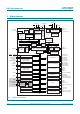
LPC2387 NXP Semiconductors Single-chip 16-bit/32-bit MCU 0xFFFF FFFF 4.0 GB AHB PERIPHERALS 0xF000 0000 3.75 GB APB PERIPHERALS 3.5 GB 0xE000 0000 3.0 GB 0xC000 0000 RESERVED ADDRESS SPACE 2.0 GB 0x8000 0000 BOOT ROM AND BOOT FLASH (BOOT FLASH REMAPPED FROM ON-CHIP FLASH) RESERVED ADDRESS SPACE 0x7FE0 3FFF 0x7FE0 0000 ETHERNET RAM (16 kB) 0x7FD0 3FFF USB RAM (16 kB) 0x7FD0 0000 RESERVED ADDRESS SPACE 0x4001 0000 0x4000 FFFF 64 kB LOCAL ON-CHIP STATIC RAM 1.
LPC2387 NXP Semiconductors Single-chip 16-bit/32-bit MCU FIQs have the highest priority. If more than one request is assigned to FIQ, the VIC ORs the requests to produce the FIQ signal to the ARM processor. The fastest possible FIQ latency is achieved when only one request is classified as FIQ, because then the FIQ service routine can simply start dealing with that device.
LPC2387 NXP Semiconductors Single-chip 16-bit/32-bit MCU • Single DMA and burst DMA request signals. Each peripheral connected to the GPDMA can assert either a burst DMA request or a single DMA request. The DMA burst size is set by programming the GPDMA. • Memory-to-memory, memory-to-peripheral, peripheral-to-memory, and peripheral-to-peripheral transfers. • Scatter or gather DMA is supported through the use of linked lists.
LPC2387 NXP Semiconductors Single-chip 16-bit/32-bit MCU Additionally, any pin on port 0 and port 2 (total of 42 pins) providing a digital function can be programmed to generate an interrupt on a rising edge, a falling edge, or both. The edge detection is asynchronous, so it may operate when clocks are not present such as during Power-down mode. Each enabled interrupt can be used to wake up the chip from Power-down mode. 7.8.
LPC2387 NXP Semiconductors Single-chip 16-bit/32-bit MCU – Receive filtering. – Multicast and broadcast frame support for both transmit and receive. – Optional automatic Frame Check Sequence (FCS) insertion with Circular Redundancy Check (CRC) for transmit. – Selectable automatic transmit frame padding. – Over-length frame support for both transmit and receive allows any length frames. – Promiscuous receive mode. – Automatic collision back-off and frame retransmission.
LPC2387 NXP Semiconductors Single-chip 16-bit/32-bit MCU • Supports DMA transfers with the DMA RAM of 8 kB on all non-control endpoints. • Allows dynamic switching between CPU-controlled and DMA modes. • Double buffer implementation for Bulk and Isochronous endpoints. 7.10.2 USB host controller The host controller enables full- and low-speed data exchange with USB devices attached to the bus. It consists of register interface, serial interface engine, and DMA controller.
LPC2387 NXP Semiconductors Single-chip 16-bit/32-bit MCU 7.11.1 Features • • • • • Two CAN controllers and buses. Data rates to 1 Mbit/s on each bus. 32-bit register and RAM access. Compatible with CAN specification 2.0B, ISO 11898-1. Global Acceptance Filter recognizes 11-bit and 29-bit receive identifiers for all CAN buses. • Acceptance Filter can provide FullCAN-style automatic reception for selected Standard Identifiers. • FullCAN messages can generate interrupts. 7.
LPC2387 NXP Semiconductors Single-chip 16-bit/32-bit MCU 7.14.1 Features • • • • 16 B Receive and Transmit FIFOs. Register locations conform to 16C550 industry standard. Receiver FIFO trigger points at 1 B, 4 B, 8 B, and 14 B. Built-in fractional baud rate generator covering wide range of baud rates without a need for external crystals of particular values. • Fractional divider for baud rate control, auto baud capabilities and FIFO control mechanism that enables software flow control implementation.
LPC2387 NXP Semiconductors Single-chip 16-bit/32-bit MCU 7.17 SD/MMC card interface The Secure Digital and Multimedia Card Interface (MCI) allows access to external SD memory cards. The SD card interface conforms to the SD Multimedia Card Specification Version 2.11. 7.17.1 Features • The MCI provides all functions specific to the SD/MMC memory card. These include the clock generation unit, power management control, and command and data transfer. • Conforms to Multimedia Card Specification v2.11.
LPC2387 NXP Semiconductors Single-chip 16-bit/32-bit MCU 7.19 I2S-bus serial I/O controllers The I2S-bus provides a standard communication interface for digital audio applications. The I2S-bus specification defines a 3-wire serial bus using one data line, one clock line, and one word select signal. The basic I2S connection has one master, which is always the master, and one slave.
LPC2387 NXP Semiconductors Single-chip 16-bit/32-bit MCU – Do nothing on match. 7.21 Pulse width modulator The PWM is based on the standard Timer block and inherits all of its features, although only the PWM function is pinned out on the LPC2387. The Timer is designed to count cycles of the system derived clock and optionally switch pins, generate interrupts or perform other actions when specified timer values occur, based on seven match registers.
LPC2387 NXP Semiconductors Single-chip 16-bit/32-bit MCU • Double edge controlled PWM outputs can be programmed to be either positive going or negative going pulses. • Match register updates are synchronized with pulse outputs to prevent generation of erroneous pulses. Software must ‘release’ new match values before they can become effective. • May be used as a standard timer if the PWM mode is not enabled. • A 32-bit Timer/Counter with a programmable 32-bit Prescaler. 7.
LPC2387 NXP Semiconductors Single-chip 16-bit/32-bit MCU • Provides Seconds, Minutes, Hours, Day of Month, Month, Year, Day of Week, and Day of Year. • Dedicated 32 kHz oscillator or programmable prescaler from APB clock. • Dedicated power supply pin can be connected to a battery or to the main 3.3 V. • Periodic interrupts can be generated from increments of any field of the time registers, and selected fractional second values. • 2 kB data SRAM powered by VBAT.
LPC2387 NXP Semiconductors Single-chip 16-bit/32-bit MCU The PLL input, in the range of 32 kHz to 25 MHz, may initially be divided down by a value ‘N’, which may be in the range of 1 to 256. This input division provides a wide range of output frequencies from the same input frequency. Following the PLL input divider is the PLL multiplier. This can multiply the input divider output through the use of a Current Controlled Oscillator (CCO) by a value ‘M’, in the range of 1 through 32768.
LPC2387 NXP Semiconductors Single-chip 16-bit/32-bit MCU The LPC2387 also implements a separate power domain in order to allow turning off power to the bulk of the device while maintaining operation of the RTC and a small SRAM, referred to as the battery RAM. 7.24.4.1 Idle mode In Idle mode, execution of instructions is suspended until either a Reset or interrupt occurs. Peripheral functions continue operation during Idle mode and may generate interrupts to cause the processor to resume execution.
LPC2387 NXP Semiconductors Single-chip 16-bit/32-bit MCU If power is supplied to the LPC2387 during Deep power-down mode, wake-up can be caused by the RTC Alarm interrupt or by external Reset. While in Deep power-down mode, external device power may be removed. In this case, the LPC2387 will start up when external power is restored.
LPC2387 NXP Semiconductors Single-chip 16-bit/32-bit MCU 7.25.2 Brownout detection The LPC2387 includes 2-stage monitoring of the voltage on the VDD(DCDC)(3V3) pins. If this voltage falls below 2.95 V, the BOD asserts an interrupt signal to the Vectored Interrupt Controller. This signal can be enabled for interrupt in the Interrupt Enable Register in the VIC in order to cause a CPU interrupt; if not, software can monitor the signal by reading a dedicated status register.
LPC2387 NXP Semiconductors Single-chip 16-bit/32-bit MCU The second AHB, referred to as AHB2, includes only the Ethernet block and an associated 16 kB SRAM. In addition, a bus bridge is provided that allows the secondary AHB to be a bus master on AHB1, allowing expansion of Ethernet buffer space into unused space in memory residing on AHB1. In summary, bus masters with access to AHB1 are the ARM7 itself, the USB block, the GPDMA function, and the Ethernet block (via the bus bridge from AHB2).
LPC2387 NXP Semiconductors Single-chip 16-bit/32-bit MCU information about processor execution to a trace port. A software debugger allows configuration of the ETM using a JTAG interface and displays the trace information that has been captured. The ETM is connected directly to the ARM core and not to the main AMBA system bus. It compresses the trace information and exports it through a narrow trace port. An external Trace Port Analyzer captures the trace information under software debugger control.
LPC2387 NXP Semiconductors Single-chip 16-bit/32-bit MCU 8. Limiting values Table 4. Limiting values In accordance with the Absolute Maximum Rating System (IEC 60134).[1] Symbol Parameter Conditions Min Max Unit VDD(3V3) supply voltage (3.3 V) core and external rail 3.0 3.6 V 3.0 3.6 V 0.5 +4.6 V 0.5 +4.6 V 0.5 +4.6 V 0.5 +5.1 V [2] 0.5 +6.0 V other I/O pins [2][3] 0.5 VDD(3V3) + 0.
LPC2387 NXP Semiconductors Single-chip 16-bit/32-bit MCU 9. Thermal characteristics The average chip junction temperature, Tj (C), can be calculated using the following equation: T j = T amb + P D R th j – a (1) • Tamb = ambient temperature (C), • Rth(j-a) = the package junction-to-ambient thermal resistance (C/W) • PD = sum of internal and I/O power dissipation The internal power dissipation is the product of IDD and VDD.
LPC2387 NXP Semiconductors Single-chip 16-bit/32-bit MCU 10. Static characteristics Table 7. Static characteristics Tamb = 40 C to +85 C for commercial applications, unless otherwise specified. Symbol Parameter Conditions Min Typ[1] Max Unit VDD(3V3) supply voltage (3.3 V) core and external rail 3.0 3.3 3.6 V VDD(DCDC)(3V3) DC-to-DC converter supply voltage (3.3 V) 3.0 3.3 3.6 V VDDA analog 3.3 V pad supply voltage 3.0 3.3 3.6 V Vi(VBAT) input voltage on pin VBAT 2.0 3.
LPC2387 NXP Semiconductors Single-chip 16-bit/32-bit MCU Table 7. Static characteristics …continued Tamb = 40 C to +85 C for commercial applications, unless otherwise specified. Symbol Parameter Conditions Min Typ[1] Max Unit Ilatch I/O latch-up current (0.5VDD(3V3)) < VI < (1.5VDD(3V3)); - - 100 mA 0 - 5.5 V Tj < 125 C input voltage VI pin configured to provide a digital function [5][6][7] [8] VO output voltage 0 - VDD(3V3) V VIH HIGH-level input voltage 2.
LPC2387 NXP Semiconductors Single-chip 16-bit/32-bit MCU Table 7. Static characteristics …continued Tamb = 40 C to +85 C for commercial applications, unless otherwise specified. Parameter Conditions Min Typ[1] Max Unit IOZ OFF-state output current 0 V < VI < 3.3 V - - 10 A VBUS bus supply voltage - - 5.25 V VDI differential input sensitivity voltage (D+) (D) 0.2 - - V VCM differential common mode voltage range includes VDI range 0.8 - 2.
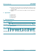
LPC2387 NXP Semiconductors Single-chip 16-bit/32-bit MCU 10.1 Power-down mode 002aae049 4 IDD(IO) (μA) 2 VDD(3V3) = 3.3 V VDD(3V3) = 3.0 V 0 −2 −4 −40 −15 10 35 60 85 temperature (°C) Vi(VBAT) = VDD(DCDC)(3V3) = 3.3 V; Tamb = 25 C. Fig 4. I/O maximum supply current IDD(IO) versus temperature in Power-down mode 002aae050 40 IBAT (μA) 30 Vi(VBAT) = 3.3 V Vi(VBAT) = 3.0 V 20 10 0 −40 −15 10 35 60 85 temperature (°C) VDD(3V3) = VDD(DCDC)(3V3) = 3.3 V; Tamb = 25 C. Fig 5.
LPC2387 NXP Semiconductors Single-chip 16-bit/32-bit MCU 002aae051 800 IDD(DCDC)pd(3v3) (μA) 600 400 VDD(DCDC)(3V3) = 3.3 V 200 0 −40 VDD(DCDC)(3V3) = 3.0 V −15 10 35 60 85 temperature (°C) VDD(3V3) = Vi(VBAT) = 3.3 V; Tamb = 25 C. Fig 6. Total DC-to-DC converter supply current IDD(DCDC)pd(3V3) at different temperatures in Power-down mode 10.2 Deep power-down mode 002aae046 300 IDD(IO) (μA) 200 100 VDD(3V3) = 3.3 V VDD(3V3) = 3.
LPC2387 NXP Semiconductors Single-chip 16-bit/32-bit MCU 002aae047 40 IBAT (μA) 30 Vi(VBAT) = 3.3 V Vi(VBAT) = 3.0 V 20 10 0 −40 −15 10 35 60 85 temperature (°C) VDD(3V3) = VDD(DCDC)(3V3) = 3.3 V; Tamb = 25 C Fig 8. RTC battery maximum supply current IBAT versus temperature in Deep power-down mode 002aae048 100 IDD(DCDC)dpd(3v3) (μA) 80 60 VDD(DCDC)(3V3) = 3.3 V 40 VDD(DCDC)(3V3) = 3.0 V 20 0 −40 −15 10 35 60 85 temperature (°C) VDD(3V3) = Vi(VBAT) = 3.3 V; Tamb = 25 C. Fig 9.
LPC2387 NXP Semiconductors Single-chip 16-bit/32-bit MCU 10.3 Electrical pin characteristics 002aaf112 3.6 VOH (V) T = 85 °C 25 °C −40 °C 3.2 2.8 2.4 2.0 0 8 16 24 IOH (mA) Conditions: VDD(3V3) = 3.3 V; standard port pins. Fig 10. Typical HIGH-level output voltage VOH versus HIGH-level output source current IOH 002aaf111 15 IOL (mA) T = 85 °C 25 °C −40 °C 10 5 0 0 0.2 0.4 0.6 VOL (V) Conditions: VDD(3V3) = 3.3 V; standard port pins. Fig 11.
LPC2387 NXP Semiconductors Single-chip 16-bit/32-bit MCU 11. Dynamic characteristics Table 8. Dynamic characteristics Tamb = 40 C to +85 C for commercial applications; VDD(3V3) over specified ranges.[1] Symbol Parameter Conditions Typ[2] Min Max Unit External clock (see Figure 12) fosc oscillator frequency 1 - 25 MHz Tcy(clk) clock cycle time 40 - 1000 ns tCHCX clock HIGH time Tcy(clk) 0.4 - - ns tCLCX clock LOW time Tcy(clk) 0.
LPC2387 NXP Semiconductors Single-chip 16-bit/32-bit MCU 11.1 Internal oscillators Table 9. Dynamic characteristic: internal oscillators Tamb = 40 C to +85 C; 3.0 V VDD(3V3) 3.6 V.[1] Symbol Parameter Conditions Min Typ[2] Max Unit fosc(RC) internal RC oscillator frequency - 3.96 4.02 4.04 MHz fi(RTC) RTC input frequency - - 32.768 - kHz Max Unit [1] Parameters are valid over operating temperature range unless otherwise specified. [2] Typical ratings are not guaranteed.
LPC2387 NXP Semiconductors Single-chip 16-bit/32-bit MCU 11.4 Flash memory Table 12. Dynamic characteristics of flash Tamb = 40 C to +85 C, unless otherwise specified; VDD(3V3) = 3.0 V to 3.6 V; all voltages are measured with respect to ground.
LPC2387 NXP Semiconductors Single-chip 16-bit/32-bit MCU 11.5 Timing TPERIOD crossover point extended crossover point differential data lines source EOP width: tFEOPT differential data to SE0/EOP skew n × TPERIOD + tFDEOP receiver EOP width: tEOPR1, tEOPR2 002aab561 Fig 13. Differential data-to-EOP transition skew and EOP width shifting edges SCK sampling edges MOSI MISO tsu(SPI_MISO) 002aad326 Fig 14.
LPC2387 NXP Semiconductors Single-chip 16-bit/32-bit MCU 12. ADC electrical characteristics Table 13. ADC electrical characteristics VDDA = 2.5 V to 3.6 V; Tamb = 40 C to +85 C unless otherwise specified; ADC frequency 4.5 MHz.
LPC2387 NXP Semiconductors Single-chip 16-bit/32-bit MCU offset error EO gain error EG 1023 1022 1021 1020 1019 1018 (2) 7 code out (1) 6 5 (5) 4 (4) 3 (3) 2 1 LSB (ideal) 1 0 1 2 3 4 5 6 7 1018 1019 1020 1021 1022 1023 1024 VIA (LSBideal) offset error EO 1 LSB = Vi(VREF) − VSSA 1024 002aae604 (1) Example of an actual transfer curve. (2) The ideal transfer curve. (3) Differential linearity error (ED). (4) Integral non-linearity (EL(adj)).
LPC2387 NXP Semiconductors Single-chip 16-bit/32-bit MCU LPC23XX 20 kΩ AD0[y] AD0[y]SAMPLE 3 pF Rvsi 5 pF VEXT VSS 002aac610 Fig 16. Suggested ADC interface - LPC2387 AD0[y] pin LPC2387 Product data sheet All information provided in this document is subject to legal disclaimers. Rev. 5.1 — 16 October 2013 © NXP B.V. 2013. All rights reserved.
LPC2387 NXP Semiconductors Single-chip 16-bit/32-bit MCU 13. DAC electrical characteristics Table 14. DAC electrical characteristics VDDA = 3.0 V to 3.6 V; Tamb = 40 C to +85 C unless otherwise specified Symbol Parameter ED Min Typ Max Unit differential linearity error - 1 - LSB EL(adj) integral non-linearity - 1.5 - LSB EO offset error - 0.6 - % EG gain error - 0.
LPC2387 NXP Semiconductors Single-chip 16-bit/32-bit MCU 14. Application information 14.1 Suggested USB interface solutions VDD(3V3) USB_UP_LED USB_CONNECT LPC23XX SoftConnect switch R1 1.5 kΩ VBUS USB_D+ RS = 33 Ω USB-B connector USB_D− RS = 33 Ω VSS 002aac578 Fig 17. LPC2387 USB interface on a self-powered device VDD(3V3) R2 LPC23XX USB_UP_LED R1 1.5 kΩ VBUS USB_D+ RS = 33 Ω USB-B connector USB_D− RS = 33 Ω VSS 002aac579 Fig 18.
LPC2387 NXP Semiconductors Single-chip 16-bit/32-bit MCU VDD R1 R2 R3 R4 RSTOUT R4 R5 VBUS ID OE_N/INT_N VDD LPC2387 RESET_N ADR/PSW SPEED SUSPEND R6 USB_SCL1 SCL USB_SDA1 SDA ISP1301 DP 33 Ω DM 33 Ω Mini-AB connector VSS INT_N EINTn USB_D+ USB_D- 002aae167 Fig 19.
LPC2387 NXP Semiconductors Single-chip 16-bit/32-bit MCU VDD USB_UP_LED VDD USB_CONNECT LPC2387 VSS USB_D+ 33 Ω D+ USB_D− 33 Ω D− VBUS USB-B connector VBUS 002aae169 Fig 21. LPC2387 USB device port configuration 14.2 Crystal oscillator XTAL input and component selection The input voltage to the on-chip oscillators is limited to 1.8 V. If the oscillator is driven by a clock in slave mode, it is recommended that the input be coupled through a capacitor with Ci = 100 pF.
LPC2387 NXP Semiconductors Single-chip 16-bit/32-bit MCU LPC2xxx L XTAL1 XTAL2 = CL CP XTAL RS CX2 CX1 002aag469 Fig 23. Oscillator modes and models: oscillation mode of operation and external crystal model used for CX1/CX2 evaluation Table 15.
LPC2387 NXP Semiconductors Single-chip 16-bit/32-bit MCU 14.3 RTC 32 kHz oscillator component selection LPC2xxx L RTCX1 RTCX2 = CL CP 32 kHz XTAL RS CX1 CX2 002aaf495 Fig 24. RTC oscillator modes and models: oscillation mode of operation and external crystal model used for CX1/CX2 evaluation The RTC external oscillator circuit is shown in Figure 24.
LPC2387 NXP Semiconductors Single-chip 16-bit/32-bit MCU 14.5 Standard I/O pin configuration Figure 25 shows the possible pin modes for standard I/O pins with analog input function: • • • • Digital output driver Digital input: Pull-up enabled/disabled Digital input: Pull-down enabled/disabled Analog input (for ADC input channels) The default configuration for standard I/O pins is input with pull-up enabled. The weak MOS devices provide a drive capability equivalent to pull-up and pull-down resistors.
LPC2387 NXP Semiconductors Single-chip 16-bit/32-bit MCU 14.6 Reset pin configuration VDD VDD VDD Rpu reset ESD 20 ns RC GLITCH FILTER PIN ESD VSS 002aaf274 Fig 26. Reset pin configuration LPC2387 Product data sheet All information provided in this document is subject to legal disclaimers. Rev. 5.1 — 16 October 2013 © NXP B.V. 2013. All rights reserved.
LPC2387 NXP Semiconductors Single-chip 16-bit/32-bit MCU 15. Package outline LQFP100: plastic low profile quad flat package; 100 leads; body 14 x 14 x 1.4 mm SOT407-1 c y X A 51 75 50 76 ZE e E HE A A2 (A 3) A1 w M θ bp Lp pin 1 index L 100 detail X 26 1 25 ZD e v M A w M bp D B HD v M B 0 5 10 mm scale DIMENSIONS (mm are the original dimensions) UNIT A max. A1 A2 A3 bp c D (1) E (1) e mm 1.6 0.15 0.05 1.45 1.35 0.25 0.27 0.17 0.20 0.09 14.1 13.9 14.1 13.
LPC2387 NXP Semiconductors Single-chip 16-bit/32-bit MCU 16. Abbreviations Table 18.
LPC2387 NXP Semiconductors Single-chip 16-bit/32-bit MCU 17. Revision history Table 19. Revision history Document ID Release date Data sheet status Change notice Supersedes LPC2387 v.5.1 20131016 Product data sheet - LPC2387 v.5 Modifications: LPC2387 v.5 Modifications: • • Product data sheet Table 8 “Dynamic characteristics”: Changed min clock cycle time from 42 to 40. 20120109 Product data sheet - LPC2387 v.
LPC2387 NXP Semiconductors Single-chip 16-bit/32-bit MCU Table 19. Revision history …continued Document ID Release date Data sheet status Change notice Supersedes LPC2387 v.4 20110210 Product data sheet - LPC2387 v.3 Modifications: LPC2387 v.3 Modifications: • • • • • • • Table 3 “Pin description”: Added Table note 9 for XTAL1 and XTAL2 pins. • • • Table 7 “Static characteristics”: Changed I2C-bus Vhys typical from 0.5VDD to 0.05VDD. • • • • • • • • • • • • • • • • • • • • Section 7.
LPC2387 NXP Semiconductors Single-chip 16-bit/32-bit MCU 18. Legal information 18.1 Data sheet status Document status[1][2] Product status[3] Definition Objective [short] data sheet Development This document contains data from the objective specification for product development. Preliminary [short] data sheet Qualification This document contains data from the preliminary specification. Product [short] data sheet Production This document contains the product specification.
LPC2387 NXP Semiconductors Single-chip 16-bit/32-bit MCU Export control — This document as well as the item(s) described herein may be subject to export control regulations. Export might require a prior authorization from competent authorities. Non-automotive qualified products — Unless this data sheet expressly states that this specific NXP Semiconductors product is automotive qualified, the product is not suitable for automotive use.
LPC2387 NXP Semiconductors Single-chip 16-bit/32-bit MCU 20. Contents 1 General description . . . . . . . . . . . . . . . . . . . . . . 1 2 Features and benefits . . . . . . . . . . . . . . . . . . . . 1 3 Applications . . . . . . . . . . . . . . . . . . . . . . . . . . . . 3 4 Ordering information . . . . . . . . . . . . . . . . . . . . . 3 4.1 Ordering options . . . . . . . . . . . . . . . . . . . . . . . . 3 5 Block diagram . . . . . . . . . . . . . . . . . . . . . . . . . . 4 6 Pinning information .
LPC2387 NXP Semiconductors Single-chip 16-bit/32-bit MCU 13 14 14.1 14.2 14.3 14.4 14.5 14.6 15 16 17 18 18.1 18.2 18.3 18.4 19 20 DAC electrical characteristics . . . . . . . . . . . . Application information. . . . . . . . . . . . . . . . . . Suggested USB interface solutions . . . . . . . . Crystal oscillator XTAL input and component selection . . . . . . . . . . . . . . . . . . . . . . . . . . . . . RTC 32 kHz oscillator component selection . .