
Datasheet

LPC2387 All information provided in this document is subject to legal disclaimers. © NXP B.V. 2013. All rights reserved.
Product data sheet Rev. 5.1 — 16 October 2013 10 of 66
NXP Semiconductors
LPC2387
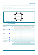
Single-chip 16-bit/32-bit MCU
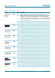
P1[27]/
USB_INT1
/
USB_OVRCR1/
CAP0[1]
43
[1]
I/O P1[27] — General purpose digital input/output pin.
I USB_INT1
— USB port 1 OTG transceiver interrupt (OTG transceiver).
I USB_OVRCR1
— USB port 1 Over-Current status.
I CAP0[1] — Capture input for Timer 0, channel 1.
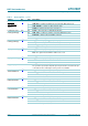
P1[28]/USB_SCL1/
PCAP1[0]/MAT0[0]
44
[1]
I/O P1[28] — General purpose digital input/output pin.
I/O USB_SCL1 — USB port 1 I
2
C-bus serial clock (OTG transceiver).
I PCAP1[0] — Capture input for PWM1, channel 0.
O MAT0[0] — Match output for Timer 0, channel 0.
P1[29]/USB_SDA1/
PCAP1[1]/MAT0[1]
45
[1]
I/O P1[29] — General purpose digital input/output pin.
I/O USB_SDA1 — USB port 1 I
2
C-bus serial data (OTG transceiver).
I PCAP1[1] — Capture input for PWM1, channel 1.
O MAT0[1] — Match output for Timer 0, channel 0.
P1[30]/V
BUS
/AD0[4] 21
[2]
I/O P1[30] — General purpose digital input/output pin.
I V
BUS
— Monitors the presence of USB bus power.
Note: This signal must be HIGH for USB reset to occur.
I AD0[4] — A/D converter 0, input 4.
P1[31]/SCK1/AD0[5] 20
[2]
I/O P1[31] — General purpose digital input/output pin.
I/O SCK1 — Serial Clock for SSP1.
I AD0[5] — A/D converter 0, input 5.
P2[0] to P2[31] I/O Port 2: Port 2 is a 32-bit I/O port with individual direction controls for each bit.
The operation of port 2 pins depends upon the pin function selected via the pin
connect block. Pins 14 through 31 of this port are not available.
P2[0]/PWM1[1]/
TXD1/TRACECLK
75
[1]
I/O P2[0] — General purpose digital input/output pin.
O PWM1[1] — Pulse Width Modulator 1, channel 1 output.
O TXD1 — Transmitter output for UART1.
O TRACECLK — Trace Clock.
P2[1]/PWM1[2]/
RXD1/PIPESTAT0
74
[1]
I/O P2[1] — General purpose digital input/output pin.
O PWM1[2] — Pulse Width Modulator 1, channel 2 output.
I RXD1 — Receiver input for UART1.
O PIPESTAT0 — Pipeline Status, bit 0.
P2[2]/PWM1[3]/
CTS1/PIPESTAT1
73
[1]
I/O P2[2] — General purpose digital input/output pin.
O PWM1[3] — Pulse Width Modulator 1, channel 3 output.
I CTS1 — Clear to Send input for UART1.
O PIPESTAT1 — Pipeline Status, bit 1.
P2[3]/PWM1[4]/
DCD1/PIPESTAT2
70
[1]
I/O P2[3] — General purpose digital input/output pin.
O PWM1[4] — Pulse Width Modulator 1, channel 4 output.
I DCD1 — Data Carrier Detect input for UART1.
O PIPESTAT2 — Pipeline Status, bit 2.
Table 3. Pin description
…continued
Symbol Pin Type Description