
Datasheet

LPC2387 All information provided in this document is subject to legal disclaimers. © NXP B.V. 2013. All rights reserved.
Product data sheet Rev. 5.1 — 16 October 2013 7 of 66
NXP Semiconductors
LPC2387
Single-chip 16-bit/32-bit MCU
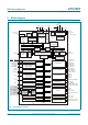
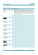
P0[17]/CTS1/
MISO0/MISO
61
[1]
I/O P0[17] — General purpose digital input/output pin.
I CTS1 — Clear to Send input for UART1.
I/O MISO0 — Master In Slave Out for SSP0.
I/O MISO — Master In Slave Out for SPI.
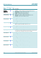
P0[18]/DCD1/
MOSI0/MOSI
60
[1]
I/O P0[18] — General purpose digital input/output pin.
I DCD1 — Data Carrier Detect input for UART1.
I/O MOSI0 — Master Out Slave In for SSP0.
I/O MOSI — Master Out Slave In for SPI.
P0[19]/DSR1/
MCICLK/SDA1
59
[1]
I/O P0[19] — General purpose digital input/output pin.
I DSR1 — Data Set Ready input for UART1.
O MCICLK — Clock output line for SD/MMC interface.
I/O SDA1 — I
2
C1 data input/output (this is not an open-drain pin).
P0[20]/DTR1/
MCICMD/SCL1
58
[1]
I/O P0[20] — General purpose digital input/output pin.
O DTR1 — Data Terminal Ready output for UART1.
I MCICMD — Command line for SD/MMC interface.
I/O SCL1 — I
2
C1 clock input/output (this is not an open-drain pin).
P0[21]/RI1/
MCIPWR/RD1
57
[1]
I/O P0[21] — General purpose digital input/output pin.
I RI1 — Ring Indicator input for UART1.
O MCIPWR — Power Supply Enable for external SD/MMC power supply.
I RD1 — CAN1 receiver input.
P0[22]/RTS1/
MCIDAT0/TD1
56
[1]
I/O P0[22] — General purpose digital input/output pin.
O RTS1 — Request to Send output for UART1.
O MCIDAT0 — Data line for SD/MMC interface.
O TD1 — CAN1 transmitter output.
P0[23]/AD0[0]/
I2SRX_CLK/
CAP3[0]
9
[2]
I/O P0[23] — General purpose digital input/output pin.
I AD0[0] — A/D converter 0, input 0.
I/O I2SRX_CLK — Receive Clock. It is driven by the master and received by the
slave. Corresponds to the signal SCK in the I
2
S-bus specification.
I CAP3[0] — Capture input for Timer 3, channel 0.
P0[24]/AD0[1]/
I2SRX_WS/
CAP3[1]
8
[2]
I/O P0[24] — General purpose digital input/output pin.
I AD0[1] — A/D converter 0, input 1.
I/O I2SRX_WS — Receive Word Select. It is driven by the master and received by
the slave. Corresponds to the signal WS in the I
2
S-bus specification.
I CAP3[1] — Capture input for Timer 3, channel 1.
P0[25]/AD0[2]/
I2SRX_SDA/
TXD3
7
[2]
I/O P0[25] — General purpose digital input/output pin.
I AD0[2] — A/D converter 0, input 2.
I/O I2SRX_SDA — Receive data. It is driven by the transmitter and read by the
receiver. Corresponds to the signal SD in the I
2
S-bus specification.
O TXD3 — Transmitter output for UART3.
Table 3. Pin description
…continued
Symbol Pin Type Description