
- NXP ARM Microcontroller Product Data Sheet

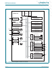


Table Of Contents
- 1. Introduction
- 2. General description
- 3. Features
- 4. Ordering information
- 5. Block diagram
- 6. Pinning information
- 7. Functional description
- 8. Block description
- 9. Limiting values
- 10. Thermal characteristics
- 11. Static characteristics
- 12. Dynamic characteristics
- 13. Package outline
- 14. Soldering
- 15. Abbreviations
- 16. References
- 17. Revision history
- 18. Legal information
- 19. Contact information
- 20. Contents

DR
AFT
DR
AFT
DRAFT
DR
D
RAFT
DRAFT
DRA
F
T DRAF
D
RAFT DRAFT DRAFT DRAFT DRAFT D
DRAFT
D
RAFT DRA
F
T DRAFT DRAFT DRAFT DRA
LPC2917_19_1 © NXP B.V. 2007. All rights reserved.
Preliminary data sheet Rev. 1.01 — 15 November 2007 19 of 68
NXP Semiconductors
LPC2917/19
ARM9 microcontroller with CAN and LIN
8.2.3 External static-memory controller pin description
The external static-memory controller module in the LPC2917/19 has the following pins,
which are combined with other functions on the port pins of the LPC2917/19. Table 12
shows the external memory controller pins.
8.2.4 External static-memory controller clock description
The External Static-Memory Controller is clocked by CLK_SYS_SMC, see Section 7.2.2.
8.2.5 External memory timing diagrams
A timing diagram for reading from external memory is shown in Figure 4. The relationship
between the wait-state settings is indicated with arrows.
Table 11. External static-memory controller banks
CS[2:0] Bank
000 bank 0
001 bank 1
010 bank 2
011 bank 3
100 bank 4
101 bank 5
110 bank 6
111 bank 7
Table 12. External memory controller pins
Symbol Direction Description
EXTBUS CSx out memory-bank x select, x runs from 0 to 7
EXTBUS BLSy out byte-lane select input y, y runs from 0 to 3
EXTBUS WE_N out write enable (active LOW)
EXTBUS OE_N out output enable (active LOW)
EXTBUS A[23:0] out address bus
EXTBUS D[31:0] in/out data bus