
- NXP ARM Microcontroller Product Data Sheet
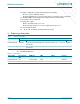
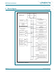


Table Of Contents
- 1. Introduction
- 2. General description
- 3. Features
- 4. Ordering information
- 5. Block diagram
- 6. Pinning information
- 7. Functional description
- 8. Block description
- 9. Limiting values
- 10. Thermal characteristics
- 11. Static characteristics
- 12. Dynamic characteristics
- 13. Package outline
- 14. Soldering
- 15. Abbreviations
- 16. References
- 17. Revision history
- 18. Legal information
- 19. Contact information
- 20. Contents

DR
AFT
DR
AFT
DRAFT
DR
D
RAFT
DRAFT
DRA
F
T DRAF
D
RAFT DRAFT DRAFT DRAFT DRAFT D
DRAFT
D
RAFT DRA
F
T DRAFT DRAFT DRAFT DRA
LPC2917_19_1 © NXP B.V. 2007. All rights reserved.
Preliminary data sheet Rev. 1.01 — 15 November 2007 6 of 68
NXP Semiconductors
LPC2917/19
ARM9 microcontroller with CAN and LIN
6. Pinning information
6.1 Pinning
6.2 Pin description
6.2.1 General description
The LPC2917/19 has up to four ports: two of 32 pins each, one of 28 pins and one of 16
pins. The pin to which each function is assigned is controlled by the SFSP registers in the
SCU. The functions combined on each port pin are shown in the pin description tables in
this section.
6.2.2 LQFP144 pin assignment
Fig 2. Pin configuration for SOT486-1 (LQFP144)
LPC2917FBD144
LPC2919FBD144
108
37
72
144
109
73
1
36
144PINS
Table 3. LQFP144 pin assignment
Symbol Pin Description
Function 0 (default) Function 1 Function 2 Function 3
TDO 1 IEEE 1149.1 test data out
P2.21 2 GPIO 2, pin 21 - PWM2 CAP1 EXTBUS D19
P0.24 3 GPIO 0, pin 24 UART1 TxD CAN1 TxD SPI2 SCS0
P0.25 4 GPIO 0, pin 25 UART1 RxD CAN1 RxD SPI2 SDO
P0.26 5 GPIO 0, pin 26 - - SPI2 SDI
P0.27 6 GPIO 0, pin 27 - - SPI2 SCK
P0.28 7 GPIO 0, pin 28 - TIMER0 CAP0 TIMER0 MAT0
P0.29 8 GPIO 0, pin 29 - TIMER0 CAP1 TIMER0 MAT1
V
DD(IO)
9 3.3 V power supply for I/O
P2.22 10 GPIO 2, pin 22 - PWM2 CAP2 EXTBUS D20
P2.23 11 GPIO 2, pin 23 - PWM3 CAP0 EXTBUS D21
P3.6 12 GPIO 3, pin 6 SPI0 SCS3 PWM1 MAT0 LIN1 TxD
P3.7 13 GPIO 3, pin 7 SPI2 SCS1 PWM1 MAT1 LIN1 RxD
P0.30 14 GPIO 0, pin 30 - TIMER0 CAP2 TIMER0 MAT2
P0.31 15 GPIO 0, pin 31 - TIMER0 CAP3 TIMER0 MAT3