LPC4350/30/20/10 32-bit ARM Cortex-M4/M0 flashless MCU; up to 264 kB SRAM; Ethernet; two HS USBs; advanced configurable peripherals Rev. 4.2 — 18 August 2014 Product data sheet 1.
LPC4350/30/20/10 NXP Semiconductors 32-bit ARM Cortex-M4/M0 microcontroller On-chip memory Up to 264 kB SRAM for code and data use. Multiple SRAM blocks with separate bus access. Two SRAM blocks can be powered down individually. 64 kB ROM containing boot code and on-chip software drivers. 64 bit + 256 bit general-purpose One-Time Programmable (OTP) memory. Clock generation unit Crystal oscillator with an operating range of 1 MHz to 25 MHz. 12 MHz Internal RC (IRC) oscillator trimmed to 1.
LPC4350/30/20/10 NXP Semiconductors 32-bit ARM Cortex-M4/M0 microcontroller Digital peripherals External Memory Controller (EMC) supporting external SRAM, ROM, NOR flash, and SDRAM devices. LCD controller with DMA support and a programmable display resolution of up to 1024 H 768 V. Supports monochrome and color STN panels and TFT color panels; supports 1/2/4/8 bpp Color Look-Up Table (CLUT) and 16/24-bit direct pixel mapping. Secure Digital Input Output (SD/MMC) card interface.
LPC4350/30/20/10 NXP Semiconductors 32-bit ARM Cortex-M4/M0 microcontroller 3. Applications LPC4350_30_20_10 Product data sheet Motor control Power management White goods RFID readers Embedded audio applications Industrial automation e-metering All information provided in this document is subject to legal disclaimers. Rev. 4.2 — 18 August 2014 © NXP Semiconductors N.V. 2014. All rights reserved.
LPC4350/30/20/10 NXP Semiconductors 32-bit ARM Cortex-M4/M0 microcontroller 4. Ordering information Table 1.
LPC4350/30/20/10 NXP Semiconductors 32-bit ARM Cortex-M4/M0 microcontroller 5.
LPC4350/30/20/10 NXP Semiconductors 32-bit ARM Cortex-M4/M0 microcontroller 6. Pinning information 6.1 Pinning LPC4350/30FET256 ball A1 index area 2 1 4 3 6 5 8 7 10 9 12 11 14 13 LPC4350/30FET180 ball A1 index area 16 2 1 15 A 4 3 6 5 8 7 10 9 12 11 A B B C C D D E E F G F J H L K G H K J M L N M P N R P T 002aag374 002aaf813 Transparent top view Transparent top view Fig 2. 14 13 Pin configuration LBGA256 package ball A1 index area Fig 3.
LPC4350/30/20/10 NXP Semiconductors 32-bit ARM Cortex-M4/M0 microcontroller Not all functions listed in Table 3 are available on all packages. See Table 2 for availability of USB0, USB1, Ethernet, and LCD functions. The parts contain two 10-bit ADCs (ADC0 and ADC1).
LPC4350/30/20/10 NXP Semiconductors 32-bit ARM Cortex-M4/M0 microcontroller Type 32 Description [1] LQFP144 G2 Reset state TFBGA100 LBGA256 Symbol TFBGA180 Table 3. Pin description LCD, Ethernet, USB0, and USB1 functions are not available on all parts. See Table 2. Multiplexed digital pins P0_0 P0_1 L3 M2 K3 K2 G1 34 [2] [2] N; PU N; PU I/O GPIO0[0] — General purpose digital input/output pin. I/O SSP1_MISO — Master In Slave Out for SSP1.
LPC4350/30/20/10 NXP Semiconductors 32-bit ARM Cortex-M4/M0 microcontroller P1_2 P1_3 P1_4 LQFP144 N1 K2 42 R3 P5 T3 LPC4350_30_20_10 Product data sheet N2 M2 P2 K1 J1 J2 43 44 47 [2] [2] [2] [2] N; PU N; PU N; PU N; PU Type TFBGA100 R2 Description [1] TFBGA180 P1_1 LBGA256 Symbol Reset state Table 3. Pin description …continued LCD, Ethernet, USB0, and USB1 functions are not available on all parts. See Table 2.
LPC4350/30/20/10 NXP Semiconductors 32-bit ARM Cortex-M4/M0 microcontroller P1_6 P1_7 LQFP144 N3 J4 48 T4 T5 P3 N4 K4 G4 49 50 [2] [2] [2] N; PU N; PU N; PU Type TFBGA100 R5 Description [1] TFBGA180 P1_5 LBGA256 Symbol Reset state Table 3. Pin description …continued LCD, Ethernet, USB0, and USB1 functions are not available on all parts. See Table 2. I/O GPIO1[8] — General purpose digital input/output pin. O CTOUT_10 — SCTimer/PWM output 10. Match output 3 of timer 3.
LPC4350/30/20/10 NXP Semiconductors 32-bit ARM Cortex-M4/M0 microcontroller P1_9 P1_10 P1_11 LQFP144 M5 H5 51 T7 R8 T9 LPC4350_30_20_10 Product data sheet N5 N6 P8 J5 H6 J7 52 53 55 [2] [2] [2] [2] N; PU N; PU N; PU N; PU Type TFBGA100 R7 Description [1] TFBGA180 P1_8 LBGA256 Symbol Reset state Table 3. Pin description …continued LCD, Ethernet, USB0, and USB1 functions are not available on all parts. See Table 2.
LPC4350/30/20/10 NXP Semiconductors 32-bit ARM Cortex-M4/M0 microcontroller P1_13 P1_14 P1_15 LQFP144 P7 K7 56 R10 R11 T12 LPC4350_30_20_10 Product data sheet L8 K7 P11 H8 J8 K8 60 61 62 [2] [2] [2] [2] N; PU N; PU N; PU N; PU Type TFBGA100 R9 Description [1] TFBGA180 P1_12 LBGA256 Symbol Reset state Table 3. Pin description …continued LCD, Ethernet, USB0, and USB1 functions are not available on all parts. See Table 2.
LPC4350/30/20/10 NXP Semiconductors 32-bit ARM Cortex-M4/M0 microcontroller P1_17 P1_18 P1_19 LQFP144 L5 H9 64 M8 N12 M11 LPC4350_30_20_10 Product data sheet L6 N10 N9 H10 66 J10 K9 67 68 [2] [3] [2] [2] N; PU N; PU N; PU N; PU Type TFBGA100 M7 Description [1] TFBGA180 P1_16 LBGA256 Symbol Reset state Table 3. Pin description …continued LCD, Ethernet, USB0, and USB1 functions are not available on all parts. See Table 2.
LPC4350/30/20/10 NXP Semiconductors 32-bit ARM Cortex-M4/M0 microcontroller P2_0 K10 70 T16 N14 G10 75 [2] [2] N; PU N; PU Type J10 Description [1] TFBGA100 M10 LQFP144 TFBGA180 P1_20 LBGA256 Symbol Reset state Table 3. Pin description …continued LCD, Ethernet, USB0, and USB1 functions are not available on all parts. See Table 2. I/O GPIO0[15] — General purpose digital input/output pin. I/O SSP1_SSEL — Slave Select for SSP1. - R — Function reserved.
LPC4350/30/20/10 NXP Semiconductors 32-bit ARM Cortex-M4/M0 microcontroller P2_3 LQFP144 L13 F5 84 J12 G11 D8 87 [2] [3] N; PU N; PU Type TFBGA100 M15 Description [1] TFBGA180 P2_2 LBGA256 Symbol Reset state Table 3. Pin description …continued LCD, Ethernet, USB0, and USB1 functions are not available on all parts. See Table 2. I/O SGPIO6 — General purpose digital input/output pin. I/O U0_UCLK — Serial clock input/output for USART0 in synchronous mode.
LPC4350/30/20/10 NXP Semiconductors 32-bit ARM Cortex-M4/M0 microcontroller D10 91 [3] N; PU Type J12 Description [1] TFBGA100 K14 LQFP144 TFBGA180 P2_5 LBGA256 Symbol Reset state Table 3. Pin description …continued LCD, Ethernet, USB0, and USB1 functions are not available on all parts. See Table 2. I/O SGPIO14 — General purpose digital input/output pin. I CTIN_2 — SCTimer/PWM input 2. Capture input 2 of timer 0. I USB1_VBUS — Monitors the presence of USB1 bus power.
LPC4350/30/20/10 NXP Semiconductors 32-bit ARM Cortex-M4/M0 microcontroller P2_9 P2_10 P2_11 LQFP144 H14 C6 98 H16 G16 F16 LPC4350_30_20_10 Product data sheet G14 F14 E13 B10 102 E8 A9 104 105 [2] [2] [2] [2] N; PU N; PU N; PU N; PU Type TFBGA100 J16 Description [1] TFBGA180 P2_8 LBGA256 Symbol Reset state Table 3. Pin description …continued LCD, Ethernet, USB0, and USB1 functions are not available on all parts. See Table 2.
LPC4350/30/20/10 NXP Semiconductors 32-bit ARM Cortex-M4/M0 microcontroller P2_13 P3_0 LQFP144 D13 B9 106 C16 F13 LPC4350_30_20_10 Product data sheet E14 D12 A10 108 A8 112 [2] [2] [2] N; PU N; PU N; PU Type TFBGA100 E15 Description [1] TFBGA180 P2_12 LBGA256 Symbol Reset state Table 3. Pin description …continued LCD, Ethernet, USB0, and USB1 functions are not available on all parts. See Table 2. I/O GPIO1[12] — General purpose digital input/output pin.
LPC4350/30/20/10 NXP Semiconductors 32-bit ARM Cortex-M4/M0 microcontroller P3_2 P3_3 LQFP144 D10 F7 114 F11 B14 LPC4350_30_20_10 Product data sheet D9 B13 G6 A7 116 118 [2] [2] [4] N; PU OL; PU N; PU Type TFBGA100 G11 Description [1] TFBGA180 P3_1 LBGA256 Symbol Reset state Table 3. Pin description …continued LCD, Ethernet, USB0, and USB1 functions are not available on all parts. See Table 2. I/O I2S0_TX_WS — Transmit Word Select.
LPC4350/30/20/10 NXP Semiconductors 32-bit ARM Cortex-M4/M0 microcontroller P3_5 P3_6 P3_7 LQFP144 C14 B8 119 C12 B13 C11 LPC4350_30_20_10 Product data sheet C11 B12 C10 B7 C7 D7 121 122 123 [2] [2] [2] [2] N; PU N; PU N; PU N; PU Type TFBGA100 A15 Description [1] TFBGA180 P3_4 LBGA256 Symbol Reset state Table 3. Pin description …continued LCD, Ethernet, USB0, and USB1 functions are not available on all parts. See Table 2.
LPC4350/30/20/10 NXP Semiconductors 32-bit ARM Cortex-M4/M0 microcontroller P4_0 P4_1 LQFP144 C9 E7 124 D5 A1 LPC4350_30_20_10 Product data sheet D4 D3 - - 1 3 [2] [2] [5] N; PU N; PU N; PU Type TFBGA100 C10 Description [1] TFBGA180 P3_8 LBGA256 Symbol Reset state Table 3. Pin description …continued LCD, Ethernet, USB0, and USB1 functions are not available on all parts. See Table 2. - R — Function reserved. I SPI_SSEL — Slave Select for SPI.
LPC4350/30/20/10 NXP Semiconductors 32-bit ARM Cortex-M4/M0 microcontroller P4_3 P4_4 LQFP144 A2 - 8 C2 B1 LPC4350_30_20_10 Product data sheet B2 A1 - - 7 9 [2] [5] [5] N; PU N; PU N; PU Type TFBGA100 D3 Description [1] TFBGA180 P4_2 LBGA256 Symbol Reset state Table 3. Pin description …continued LCD, Ethernet, USB0, and USB1 functions are not available on all parts. See Table 2. I/O GPIO2[2] — General purpose digital input/output pin. O CTOUT_0 — SCTimer/PWM output 0.
LPC4350/30/20/10 NXP Semiconductors 32-bit ARM Cortex-M4/M0 microcontroller P4_6 P4_7 P4_8 LQFP144 C2 - 10 C1 H4 E2 LPC4350_30_20_10 Product data sheet B1 F4 D2 - - - 11 14 15 [2] [2] [2] [2] N; PU N; PU O; PU N; PU Type TFBGA100 D2 Description [1] TFBGA180 P4_5 LBGA256 Symbol Reset state Table 3. Pin description …continued LCD, Ethernet, USB0, and USB1 functions are not available on all parts. See Table 2. I/O GPIO2[5] — General purpose digital input/output pin.
LPC4350/30/20/10 NXP Semiconductors 32-bit ARM Cortex-M4/M0 microcontroller P4_10 P5_0 P5_1 LQFP144 J2 - 33 M3 N3 P3 LPC4350_30_20_10 Product data sheet L3 L2 M1 - - - 35 37 39 [2] [2] [2] [2] N; PU N; PU N; PU N; PU Type TFBGA100 L2 Description [1] TFBGA180 P4_9 LBGA256 Symbol Reset state Table 3. Pin description …continued LCD, Ethernet, USB0, and USB1 functions are not available on all parts. See Table 2. - R — Function reserved.
LPC4350/30/20/10 NXP Semiconductors 32-bit ARM Cortex-M4/M0 microcontroller P5_3 P5_4 P5_5 LQFP144 M3 - 46 T8 P9 P10 LPC4350_30_20_10 Product data sheet P6 N7 N8 - - - 54 57 58 [2] [2] [2] [2] N; PU N; PU N; PU N; PU Type TFBGA100 R4 Description [1] TFBGA180 P5_2 LBGA256 Symbol Reset state Table 3. Pin description …continued LCD, Ethernet, USB0, and USB1 functions are not available on all parts. See Table 2.
LPC4350/30/20/10 NXP Semiconductors 32-bit ARM Cortex-M4/M0 microcontroller P5_7 P6_0 P6_1 LQFP144 M11 - 63 R12 M12 R15 LPC4350_30_20_10 Product data sheet N11 M10 P14 - H7 G5 65 73 74 [2] [2] [2] [2] N; PU N; PU N; PU N; PU Type TFBGA100 T13 Description [1] TFBGA180 P5_6 LBGA256 Symbol Reset state Table 3. Pin description …continued LCD, Ethernet, USB0, and USB1 functions are not available on all parts. See Table 2.
LPC4350/30/20/10 NXP Semiconductors 32-bit ARM Cortex-M4/M0 microcontroller P6_3 LQFP144 K11 J9 78 P15 N13 - 79 [2] [2] N; PU N; PU Type TFBGA100 L13 Description [1] TFBGA180 P6_2 LBGA256 Symbol Reset state Table 3. Pin description …continued LCD, Ethernet, USB0, and USB1 functions are not available on all parts. See Table 2. I/O GPIO3[1] — General purpose digital input/output pin. O EMC_CKEOUT1 — SDRAM clock enable 1.
LPC4350/30/20/10 NXP Semiconductors 32-bit ARM Cortex-M4/M0 microcontroller P6_6 P6_7 P6_8 LQFP144 L14 F9 82 L14 J13 H13 LPC4350_30_20_10 Product data sheet K12 H11 F12 - - - 83 85 86 [2] [2] [2] [2] N; PU N; PU N; PU N; PU Type TFBGA100 P16 Description [1] TFBGA180 P6_5 LBGA256 Symbol Reset state Table 3. Pin description …continued LCD, Ethernet, USB0, and USB1 functions are not available on all parts. See Table 2.
LPC4350/30/20/10 NXP Semiconductors 32-bit ARM Cortex-M4/M0 microcontroller P6_10 P6_11 P6_12 LQFP144 H13 F8 97 H15 H12 G15 LPC4350_30_20_10 Product data sheet G13 F11 F13 - C9 - 100 101 103 [2] [2] [2] [2] N; PU N; PU N; PU N; PU Type TFBGA100 J15 Description [1] TFBGA180 P6_9 LBGA256 Symbol Reset state Table 3. Pin description …continued LCD, Ethernet, USB0, and USB1 functions are not available on all parts. See Table 2.
LPC4350/30/20/10 NXP Semiconductors 32-bit ARM Cortex-M4/M0 microcontroller P7_1 P7_2 P7_3 LQFP144 B14 - 110 C14 A16 C13 LPC4350_30_20_10 Product data sheet C13 A14 C12 - - - 113 115 117 [2] [2] [2] [2] N; PU N; PU N; PU N; PU Type TFBGA100 B16 Description [1] TFBGA180 P7_0 LBGA256 Symbol Reset state Table 3. Pin description …continued LCD, Ethernet, USB0, and USB1 functions are not available on all parts. See Table 2.
LPC4350/30/20/10 NXP Semiconductors 32-bit ARM Cortex-M4/M0 microcontroller P7_5 P7_6 LQFP144 C6 - 132 A7 C7 LPC4350_30_20_10 Product data sheet A7 F5 - - 133 134 [5] [5] [2] N; PU N; PU N; PU Type TFBGA100 C8 Description [1] TFBGA180 P7_4 LBGA256 Symbol Reset state Table 3. Pin description …continued LCD, Ethernet, USB0, and USB1 functions are not available on all parts. See Table 2. I/O GPIO3[12] — General purpose digital input/output pin.
LPC4350/30/20/10 NXP Semiconductors 32-bit ARM Cortex-M4/M0 microcontroller P8_0 P8_1 P8_2 LQFP144 D5 - 140 E5 H5 K4 LPC4350_30_20_10 Product data sheet E4 G4 J4 - - - - - - [5] [3] [3] [3] N; PU N; PU N; PU N; PU Type TFBGA100 B6 Description [1] TFBGA180 P7_7 LBGA256 Symbol Reset state Table 3. Pin description …continued LCD, Ethernet, USB0, and USB1 functions are not available on all parts. See Table 2. I/O GPIO3[15] — General purpose digital input/output pin.
LPC4350/30/20/10 NXP Semiconductors 32-bit ARM Cortex-M4/M0 microcontroller P8_4 P8_5 P8_6 LQFP144 H3 - - J2 J1 K3 LPC4350_30_20_10 Product data sheet H2 H1 J3 - - - - - - [2] [2] [2] [2] N; PU N; PU N; PU N; PU Type TFBGA100 J3 Description [1] TFBGA180 P8_3 LBGA256 Symbol Reset state Table 3. Pin description …continued LCD, Ethernet, USB0, and USB1 functions are not available on all parts. See Table 2. I/O GPIO4[3] — General purpose digital input/output pin.
LPC4350/30/20/10 NXP Semiconductors 32-bit ARM Cortex-M4/M0 microcontroller P8_8 P9_0 P9_1 LQFP144 J1 - - L1 T1 N6 LPC4350_30_20_10 Product data sheet K1 P1 P4 - - - - - - [2] [2] [2] [2] N; PU N; PU N; PU N; PU Type TFBGA100 K1 Description [1] TFBGA180 P8_7 LBGA256 Symbol Reset state Table 3. Pin description …continued LCD, Ethernet, USB0, and USB1 functions are not available on all parts. See Table 2. I/O GPIO4[7] — General purpose digital input/output pin.
LPC4350/30/20/10 NXP Semiconductors 32-bit ARM Cortex-M4/M0 microcontroller P9_3 P9_4 P9_5 LQFP144 M6 - - M6 N10 M9 P5 M8 L7 - - - - - 69 [2] [2] [2] [2] N; PU N; PU N; PU N; PU Type TFBGA100 N8 Description [1] TFBGA180 P9_2 LBGA256 Symbol Reset state Table 3. Pin description …continued LCD, Ethernet, USB0, and USB1 functions are not available on all parts. See Table 2. I/O GPIO4[14] — General purpose digital input/output pin.
LPC4350/30/20/10 NXP Semiconductors 32-bit ARM Cortex-M4/M0 microcontroller PA_0 PA_1 PA_2 LQFP144 M9 - 72 L12 J14 K15 LPC4350_30_20_10 Product data sheet L10 H12 J13 - - - - - - [2] [2] [3] [3] N; PU N; PU N; PU N; PU Type TFBGA100 L11 Description [1] TFBGA180 P9_6 LBGA256 Symbol Reset state Table 3. Pin description …continued LCD, Ethernet, USB0, and USB1 functions are not available on all parts. See Table 2.
LPC4350/30/20/10 NXP Semiconductors 32-bit ARM Cortex-M4/M0 microcontroller PA_4 PB_0 PB_1 LQFP144 E10 - - G13 B15 A14 LPC4350_30_20_10 Product data sheet E12 D14 A13 - - - - - - [3] [2] [2] [2] N; PU N; PU N; PU N; PU Type TFBGA100 H11 Description [1] TFBGA180 PA_3 LBGA256 Symbol Reset state Table 3. Pin description …continued LCD, Ethernet, USB0, and USB1 functions are not available on all parts. See Table 2.
LPC4350/30/20/10 NXP Semiconductors 32-bit ARM Cortex-M4/M0 microcontroller PB_3 PB_4 PB_5 LQFP144 B11 - - A13 B11 A12 LPC4350_30_20_10 Product data sheet A12 B10 A11 - - - - - - [2] [2] [2] [2] N; PU N; PU N; PU N; PU Type TFBGA100 B12 Description [1] TFBGA180 PB_2 LBGA256 Symbol Reset state Table 3. Pin description …continued LCD, Ethernet, USB0, and USB1 functions are not available on all parts. See Table 2. - R — Function reserved.
LPC4350/30/20/10 NXP Semiconductors 32-bit ARM Cortex-M4/M0 microcontroller PC_0 PC_1 PC_2 LQFP144 C5 - - D4 E4 F6 LPC4350_30_20_10 Product data sheet - - - - - - - - - [5] [5] [2] [2] N; PU N; PU N; PU N; PU Type TFBGA100 A6 Description [1] TFBGA180 PB_6 LBGA256 Symbol Reset state Table 3. Pin description …continued LCD, Ethernet, USB0, and USB1 functions are not available on all parts. See Table 2. - R — Function reserved.
LPC4350/30/20/10 NXP Semiconductors 32-bit ARM Cortex-M4/M0 microcontroller PC_4 LQFP144 - - - F4 - - - [5] [2] N; PU N; PU Type TFBGA100 F5 Description [1] TFBGA180 PC_3 LBGA256 Symbol Reset state Table 3. Pin description …continued LCD, Ethernet, USB0, and USB1 functions are not available on all parts. See Table 2. I/O USB1_ULPI_D5 — ULPI link bidirectional data line 5. - R — Function reserved. O U1_RTS — Request to Send output for UART 1.
LPC4350/30/20/10 NXP Semiconductors 32-bit ARM Cortex-M4/M0 microcontroller PC_8 PC_9 PC_10 LQFP144 - - - N4 K2 M5 LPC4350_30_20_10 Product data sheet - - - - - - - - - [2] [2] [2] [2] N; PU N; PU N; PU N; PU Type TFBGA100 G5 Description [1] TFBGA180 PC_7 LBGA256 Symbol Reset state Table 3. Pin description …continued LCD, Ethernet, USB0, and USB1 functions are not available on all parts. See Table 2. - R — Function reserved.
LPC4350/30/20/10 NXP Semiconductors 32-bit ARM Cortex-M4/M0 microcontroller PC_12 PC_13 PC_14 LQFP144 - - - L6 M1 N1 LPC4350_30_20_10 Product data sheet - - - - - - - - - [2] [2] [2] [2] N; PU N; PU N; PU N; PU Type TFBGA100 L5 Description [1] TFBGA180 PC_11 LBGA256 Symbol Reset state Table 3. Pin description …continued LCD, Ethernet, USB0, and USB1 functions are not available on all parts. See Table 2. - R — Function reserved.
LPC4350/30/20/10 NXP Semiconductors 32-bit ARM Cortex-M4/M0 microcontroller PD_1 PD_2 PD_3 LQFP144 - - - P1 R1 P4 LPC4350_30_20_10 Product data sheet - - - - - - - - - [2] [2] [2] [2] N; PU N; PU N; PU N; PU Type TFBGA100 N2 Description [1] TFBGA180 PD_0 LBGA256 Symbol Reset state Table 3. Pin description …continued LCD, Ethernet, USB0, and USB1 functions are not available on all parts. See Table 2. - R — Function reserved. O CTOUT_15 — SCTimer/PWM output 15.
LPC4350/30/20/10 NXP Semiconductors 32-bit ARM Cortex-M4/M0 microcontroller PD_5 PD_6 PD_7 LQFP144 - - - P6 R6 T6 LPC4350_30_20_10 Product data sheet - - - - - - - - - [2] [2] [2] [2] N; PU N; PU N; PU N; PU Type TFBGA100 T2 Description [1] TFBGA180 PD_4 LBGA256 Symbol Reset state Table 3. Pin description …continued LCD, Ethernet, USB0, and USB1 functions are not available on all parts. See Table 2. - R — Function reserved. O CTOUT_8 — SCTimer/PWM output 8.
LPC4350/30/20/10 NXP Semiconductors 32-bit ARM Cortex-M4/M0 microcontroller PD_9 PD_10 PD_11 LQFP144 - - - T11 P11 N9 LPC4350_30_20_10 Product data sheet - - M7 - - - - - - [2] [2] [2] [2] N; PU N; PU N; PU N; PU Type TFBGA100 P8 Description [1] TFBGA180 PD_8 LBGA256 Symbol Reset state Table 3. Pin description …continued LCD, Ethernet, USB0, and USB1 functions are not available on all parts. See Table 2. - R — Function reserved. I CTIN_6 — SCTimer/PWM input 6.
LPC4350/30/20/10 NXP Semiconductors 32-bit ARM Cortex-M4/M0 microcontroller PD_13 PD_14 PD_15 LQFP144 P9 - - T14 R13 T15 LPC4350_30_20_10 Product data sheet - L11 P13 - - - - - - [2] [2] [2] N; PU N; PU N; PU [2] N; PU Type TFBGA100 N11 Description [1] TFBGA180 PD_12 LBGA256 Symbol Reset state Table 3. Pin description …continued LCD, Ethernet, USB0, and USB1 functions are not available on all parts. See Table 2. - R — Function reserved. - R — Function reserved.
LPC4350/30/20/10 NXP Semiconductors 32-bit ARM Cortex-M4/M0 microcontroller PE_0 PE_1 PE_2 LQFP144 P12 - - P14 N14 M14 LPC4350_30_20_10 Product data sheet N12 M12 L12 - - - - - - [2] [2] [2] [2] N; PU N; PU N; PU N; PU Type TFBGA100 R14 Description [1] TFBGA180 PD_16 LBGA256 Symbol Reset state Table 3. Pin description …continued LCD, Ethernet, USB0, and USB1 functions are not available on all parts. See Table 2. - R — Function reserved. - R — Function reserved.
LPC4350/30/20/10 NXP Semiconductors 32-bit ARM Cortex-M4/M0 microcontroller PE_4 PE_5 PE_6 LQFP144 K10 - - K13 N16 M16 LPC4350_30_20_10 Product data sheet J11 - - - - - - - - [2] [2] [2] [2] N; PU N; PU N; PU N; PU Type TFBGA100 K12 Description [1] TFBGA180 PE_3 LBGA256 Symbol Reset state Table 3. Pin description …continued LCD, Ethernet, USB0, and USB1 functions are not available on all parts. See Table 2. - R — Function reserved.
LPC4350/30/20/10 NXP Semiconductors 32-bit ARM Cortex-M4/M0 microcontroller PE_8 PE_9 PE_10 LQFP144 - - - F14 E16 E14 LPC4350_30_20_10 Product data sheet - - - - - - - - - [2] [2] [2] [2] N; PU N; PU N; PU N; PU Type TFBGA100 F15 Description [1] TFBGA180 PE_7 LBGA256 Symbol Reset state Table 3. Pin description …continued LCD, Ethernet, USB0, and USB1 functions are not available on all parts. See Table 2. - R — Function reserved. O CTOUT_5 — SCTimer/PWM output 5.
LPC4350/30/20/10 NXP Semiconductors 32-bit ARM Cortex-M4/M0 microcontroller PE_12 PE_13 PE_14 LQFP144 - - - D15 G14 C15 LPC4350_30_20_10 Product data sheet - - - - - - - - - [2] [2] [2] [2] N; PU N; PU N; PU N; PU Type TFBGA100 D16 Description [1] TFBGA180 PE_11 LBGA256 Symbol Reset state Table 3. Pin description …continued LCD, Ethernet, USB0, and USB1 functions are not available on all parts. See Table 2. - R — Function reserved.
LPC4350/30/20/10 NXP Semiconductors 32-bit ARM Cortex-M4/M0 microcontroller PF_0 PF_1 PF_2 LQFP144 - - - D12 E11 D11 LPC4350_30_20_10 Product data sheet - - - - - - - - - [2] [2] [2] [2] N; PU O; PU N; PU N; PU Type TFBGA100 E13 Description [1] TFBGA180 PE_15 LBGA256 Symbol Reset state Table 3. Pin description …continued LCD, Ethernet, USB0, and USB1 functions are not available on all parts. See Table 2. - R — Function reserved. O CTOUT_0 — SCTimer/PWM output 0.
LPC4350/30/20/10 NXP Semiconductors 32-bit ARM Cortex-M4/M0 microcontroller PF_4 PF_5 LQFP144 - - - D10 E9 LPC4350_30_20_10 Product data sheet D6 - H4 - 120 - [2] [2] [5] N; PU O; PU N; PU Type TFBGA100 E10 Description [1] TFBGA180 PF_3 LBGA256 Symbol Reset state Table 3. Pin description …continued LCD, Ethernet, USB0, and USB1 functions are not available on all parts. See Table 2. - R — Function reserved. I U3_RXD — Receiver input for USART3.
LPC4350/30/20/10 NXP Semiconductors 32-bit ARM Cortex-M4/M0 microcontroller PF_7 PF_8 LQFP144 - - - B7 E6 LPC4350_30_20_10 Product data sheet - - - - - - [5] [5] [5] N; PU N; PU N; PU Type TFBGA100 E7 Description [1] TFBGA180 PF_6 LBGA256 Symbol Reset state Table 3. Pin description …continued LCD, Ethernet, USB0, and USB1 functions are not available on all parts. See Table 2. - R — Function reserved.
LPC4350/30/20/10 NXP Semiconductors 32-bit ARM Cortex-M4/M0 microcontroller PF_10 PF_11 LQFP144 - - - A3 A2 LPC4350_30_20_10 Product data sheet - - - - - - [5] [5] [5] N; PU N; PU N; PU Type TFBGA100 D6 Description [1] TFBGA180 PF_9 LBGA256 Symbol Reset state Table 3. Pin description …continued LCD, Ethernet, USB0, and USB1 functions are not available on all parts. See Table 2. - R — Function reserved.
LPC4350/30/20/10 NXP Semiconductors 32-bit ARM Cortex-M4/M0 microcontroller TFBGA100 LQFP144 M4 K3 45 Type TFBGA180 N5 Description [1] LBGA256 Symbol Reset state Table 3. Pin description …continued LCD, Ethernet, USB0, and USB1 functions are not available on all parts. See Table 2. Clock pins CLK0 CLK1 CLK2 CLK3 T10 D14 P12 LPC4350_30_20_10 Product data sheet - P10 - - K6 - - 99 - [4] [4] [4] [4] O; PU O; PU O; PU O; PU O EMC_CLK0 — SDRAM clock 0.
LPC4350/30/20/10 NXP Semiconductors 32-bit ARM Cortex-M4/M0 microcontroller TFBGA100 LQFP144 K4 A6 28 Type TFBGA180 L4 Description [1] LBGA256 Symbol Reset state Table 3. Pin description …continued LCD, Ethernet, USB0, and USB1 functions are not available on all parts. See Table 2. Debug pins DBGEN [2] I; PU I JTAG interface control signal. Also used for boundary scan. To use the part in functional mode, connect this pin in one of the following ways: • Leave DBGEN open.
LPC4350/30/20/10 NXP Semiconductors 32-bit ARM Cortex-M4/M0 microcontroller LQFP144 A10 C8 - - [11] I; IA I External wake-up input; can raise an interrupt and can cause wake-up from any of the low-power modes. A pulse with a duration > 45 ns wakes up the part. This pin does not have an internal pull-up. WAKEUP2 C9 E5 - - [11] I; IA I External wake-up input; can raise an interrupt and can cause wake-up from any of the low-power modes. A pulse with a duration > 45 ns wakes up the part.
LPC4350/30/20/10 NXP Semiconductors 32-bit ARM Cortex-M4/M0 microcontroller Table 3. Pin description …continued LCD, Ethernet, USB0, and USB1 functions are not available on all parts. See Table 2. LQFP144 Reset state G3 F3 D2 17 - - USB 3.3 V separate power supply voltage. USB0_VSSA _TERM H3 G3 D3 19 - - Dedicated analog ground for clean reference for termination resistors.
LPC4350/30/20/10 NXP Semiconductors 32-bit ARM Cortex-M4/M0 microcontroller VSSIO VSSA C4, D13, G6, G7, G8, H8, H9, J8, J9, K9, K10, M13, P7, P13 C8, D4, D5, G8, J3, J6 4, 40, 76, 109 B2 A3 C2 B9 B8 - [13] Type Description [1] Reset state LQFP144 TFBGA100 LBGA256 Symbol TFBGA180 Table 3. Pin description …continued LCD, Ethernet, USB0, and USB1 functions are not available on all parts. See Table 2. - - Ground. 135 - - Analog ground. - - - n.c.
LPC4350/30/20/10 NXP Semiconductors 32-bit ARM Cortex-M4/M0 microcontroller 7. Functional description 7.1 Architectural overview The ARM Cortex-M4 includes three AHB-Lite buses: the system bus, the I-CODE bus, and the D-code bus. The I-CODE and D-code core buses allow for concurrent code and data accesses from different slave ports.
LPC4350/30/20/10 NXP Semiconductors 32-bit ARM Cortex-M4/M0 microcontroller 7.
LPC4350/30/20/10 NXP Semiconductors 32-bit ARM Cortex-M4/M0 microcontroller 7.6.1 Features • • • • • • Controls system exceptions and peripheral interrupts. The Cortex-M4 NVIC supports up to 53 vectored interrupts. Eight programmable interrupt priority levels with hardware priority level masking. Relocatable vector table. Non-Maskable Interrupt (NMI). Software interrupt generation. 7.6.
LPC4350/30/20/10 NXP Semiconductors 32-bit ARM Cortex-M4/M0 microcontroller 7.9.1 Features • • • • • Single selection of a source. Signal inversion. Can capture a pulse if the input event source is faster than the target clock. Synchronization of input event and target clock. Single-cycle pulse generation for target. 7.
LPC4350/30/20/10 NXP Semiconductors 32-bit ARM Cortex-M4/M0 microcontroller Table 4. Boot mode when OTP BOOT_SRC bits are programmed …continued Boot mode BOOT_SRC BOOT_SRC BOOT_SRC bit 3 bit 2 bit 1 BOOT_SRC Description bit 0 EMC 16-bit 0 1 0 0 Boot from external static memory (such as NOR flash) using CS0 and a 16-bit data bus. EMC 32-bit 0 1 0 1 Boot from external static memory (such as NOR flash) using CS0 and a 32-bit data bus. USB0 0 1 1 0 Boot from USB0.
LPC4350/30/20/10 NXP Semiconductors 32-bit ARM Cortex-M4/M0 microcontroller LPC4350/30/20/10 4 GB 0xFFFF FFFF reserved 0xE010 0000 ARM private bus 0xE000 0000 reserved 0x8800 0000 SPIFI data 0x8000 0000 256 MB dynamic external memory DYCS3 256 MB dynamic external memory DYCS2 reserved 0x7000 0000 0x6000 0000 0x4400 0000 peripheral bit band alias region reserved 0x4200 0000 0x4010 2000 SGPIO 0x4010 1000 SPI 0x4010 0000 reserved 0x400F 8000 high-speed GPIO 0x400F 4000 reserved 0x400F 20
xxxxxxxxxxxxxxxxxxxxx xxxxxxxxxxxxxxxxxxxxxxxxxx xxxxxxx x x x xxxxxxxxxxxxxxxxxxxxxxxxxxxxxx xxxxxxxxxxxxxxxxxxx xx xx xxxxx xxxxxxxxxxxxxxxxxxxxxxxxxxx xxxxxxxxxxxxxxxxxxx xxxxxx xxxxxxxxxxxxxxxxxxxxxxxxxxxxxxxxxxx xxxxxxxxxxxx x x xxxxxxxxxxxxxxxxxxxxx xxxxxxxxxxxxxxxxxxxxxxxxxxxxxx xxxxx xxxxxxxxxxxxxxxxxxxxxxxxxxxxxxxxxxxxxxxxxxxxxxxxxx xxxxxxxx xxxxxxxxxxxxxxxxxxxxxxxxx xxxxxxxxxxxxxxxxxxxx xxx 0x400E 5000 reserved 0x400E 4000 ADC1 0x400E 3000 ADC0 0x400E 2000 C_CAN0 0x400E 1000 DAC 0x400E
LPC4350/30/20/10 NXP Semiconductors 32-bit ARM Cortex-M4/M0 microcontroller 7.14 One-Time Programmable (OTP) memory The OTP provides 64 bit + 256 bit One-Time Programmable (OTP) memory for general-purpose use. 7.15 General-Purpose I/O (GPIO) The LPC4350/30/20/10 provide eight GPIO ports with up to 31 GPIO pins each. Device pins that are not connected to a specific peripheral function are controlled by the GPIO registers. Pins may be dynamically configured as inputs or outputs.
LPC4350/30/20/10 NXP Semiconductors 32-bit ARM Cortex-M4/M0 microcontroller In the two-counter case, the following operational elements are global to the SCTimer/PWM, but the last three can use match conditions from either counter: • • • • • 7.16.1.1 Clock selection Inputs Events Outputs Interrupts Features • • • • • • • • Two 16-bit counters or one 32-bit counter. Counters clocked by bus clock or selected input. Counters can be configured as up-counters or up-down counters.
LPC4350/30/20/10 NXP Semiconductors 32-bit ARM Cortex-M4/M0 microcontroller 7.17 AHB peripherals 7.17.1 General-Purpose DMA (GPDMA) The DMA controller allows peripheral-to memory, memory-to-peripheral, peripheral-to-peripheral, and memory-to-memory transactions. Each DMA stream provides unidirectional serial DMA transfers for a single source and destination. For example, a bidirectional port requires one stream for transmit and one for receives.
LPC4350/30/20/10 NXP Semiconductors 32-bit ARM Cortex-M4/M0 microcontroller After a few commands configure the interface at startup, the entire flash content is accessible as normal memory using byte, halfword, and word accesses by the processor and/or DMA channels. Simple sequences of commands handle erasing and programming.
LPC4350/30/20/10 NXP Semiconductors 32-bit ARM Cortex-M4/M0 microcontroller – Output enable and write enable delays – Extended wait • Four chip selects for synchronous memory and four chip selects for static memory devices. • Power-saving modes dynamically control EMC_CKEOUT and EMC_CLK signals to SDRAMs. • Dynamic memory self-refresh mode controlled by software. • Controller supports 2048 (A0 to A10), 4096 (A0 to A11), and 8192 (A0 to A12) row address synchronous memory parts.
LPC4350/30/20/10 NXP Semiconductors 32-bit ARM Cortex-M4/M0 microcontroller • Supports auto USB 2.0 mode discovery. • Supports all high-speed USB-compliant peripherals if connected to external ULPI PHY. • • • • Supports all full-speed USB-compliant peripherals. Supports interrupts. This module has its own, integrated DMA engine. USB interface electrical test software included in ROM USB stack. 7.17.7 LCD controller Remark: The LCD controller is available on LPC4350 only. See Table 2.
LPC4350/30/20/10 NXP Semiconductors 32-bit ARM Cortex-M4/M0 microcontroller • LCD panel clock may be generated from the peripheral clock, or from a clock input pin. 7.17.8 Ethernet Remark: The Ethernet peripheral is available on parts LPC4350/30. See Table 2. 7.17.8.1 Features • • • • 10/100 Mbit/s DMA support Power management remote wake-up frame and magic packet detection Supports both full-duplex and half-duplex operation – Supports CSMA/CD Protocol for half-duplex operation. – Supports IEEE 802.
LPC4350/30/20/10 NXP Semiconductors 32-bit ARM Cortex-M4/M0 microcontroller • DMA support. 7.18.2 USART0/2/3 The LPC4350/30/20/10 contain three USARTs. In addition to standard transmit and receive data lines, the USARTs support a synchronous mode. The USARTs include a fractional baud rate generator. Standard baud rates such as 115200 Bd can be achieved with any crystal frequency above 2 MHz. 7.18.2.1 Features • • • • • Maximum UART data bit rate of 8 MBit/s. 16 B Receive and Transmit FIFOs.
LPC4350/30/20/10 NXP Semiconductors 32-bit ARM Cortex-M4/M0 microcontroller transfers, with frames of 4 bit to 16 bit of data flowing from the master to the slave and from the slave to the master. In practice, often only one of these data flows carries meaningful data. 7.18.4.1 Features • Maximum SSP speed in full-duplex mode of 25 Mbit/s; for transmit only 50 Mbit/s (master) and 17 Mbit/s (slave).
LPC4350/30/20/10 NXP Semiconductors 32-bit ARM Cortex-M4/M0 microcontroller The I2S-bus provides a standard communication interface for digital audio applications. The I2S-bus specification defines a 3-wire serial bus using one data line, one clock line, and one word select signal. The basic I2S-bus connection has one master, which is always the master, and one slave. The I2S-bus interface provides a separate transmit and receive channel, each of which can operate as either a master or a slave. 7.18.6.
LPC4350/30/20/10 NXP Semiconductors 32-bit ARM Cortex-M4/M0 microcontroller 7.19 Counter/timers and motor control 7.19.1 General purpose 32-bit timers/external event counters The LPC4350/30/20/10 include four 32-bit timer/counters. The timer/counter is designed to count cycles of the system derived clock or an externally-supplied clock. It can optionally generate interrupts, generate timed DMA requests, or perform other actions at specified timer values, based on four match registers.
LPC4350/30/20/10 NXP Semiconductors 32-bit ARM Cortex-M4/M0 microcontroller • • • • • • • • • Increments/decrements depending on direction. Programmable for 2 or 4 position counting. Velocity capture using built-in timer. Velocity compare function with “less than” interrupt. Uses 32-bit registers for position and velocity. Three position-compare registers with interrupts. Index counter for revolution counting. Index compare register with interrupts.
LPC4350/30/20/10 NXP Semiconductors 32-bit ARM Cortex-M4/M0 microcontroller • Selectable time period from (Tcy(WDCLK) 256 4) to (Tcy(WDCLK) 224 4) in multiples of Tcy(WDCLK) 4. • The Watchdog Clock (WDCLK) uses the IRC as the clock source. 7.20 Analog peripherals 7.20.1 Analog-to-Digital Converter (ADC0/1) 7.20.1.1 Features • • • • • • • 10-bit successive approximation analog to digital converter. Input multiplexing among 8 pins. Power-down mode. Measurement range 0 to VDDA.
LPC4350/30/20/10 NXP Semiconductors 32-bit ARM Cortex-M4/M0 microcontroller • Calibration counter allows adjustment to better than 1 sec/day with 1 sec resolution. • Periodic interrupts can be generated from increments of any field of the time registers. • Alarm interrupt can be generated for a specific date/time. 7.21.2 Alarm timer The alarm timer is a 16-bit timer and counts down at 1 kHz from a preset value generating alarms in intervals of up to 1 min.
LPC4350/30/20/10 NXP Semiconductors 32-bit ARM Cortex-M4/M0 microcontroller 7.22.4 Internal RC oscillator (IRC) The IRC is used as the clock source for the WWDT and/or as the clock that drives the PLLs and the CPU. The nominal IRC frequency is 12 MHz. The IRC is trimmed to 1.5 % accuracy over the entire voltage and temperature range. Upon power-up or any chip reset, the LPC4350/30/20/10 use the IRC as the clock source.
LPC4350/30/20/10 NXP Semiconductors 32-bit ARM Cortex-M4/M0 microcontroller LPC43xx to I/O pads VDDIO to cores VSS REGULATOR to memories, peripherals, oscillators, PLLs VDDREG MAIN POWER DOMAIN ULTRA LOW-POWER REGULATOR VBAT to RTC domain peripherals RESET WAKEUP0/1/2/3 RESET/WAKE-UP CONTROL to RTC I/O pads (Vps) BACKUP REGISTERS RTCX1 32 kHz OSCILLATOR RTCX2 ALARM REAL-TIME CLOCK ALWAYS-ON/RTC POWER DOMAIN DAC VDDA VSSA ADC ADC POWER DOMAIN OTP VPP OTP POWER DOMAIN USB0_VDDA3V_DRIVER
LPC4350/30/20/10 NXP Semiconductors 32-bit ARM Cortex-M4/M0 microcontroller Active mode and sleep mode apply to the state of the core. In a dual-core system, either core can be in active or sleep mode independently of the other core. If the core is in Active mode, it is fully operational and can access peripherals and memories as configured by software. If the core is in Sleep mode, it receives no clocks, but peripherals and memories remain running.
LPC4350/30/20/10 NXP Semiconductors 32-bit ARM Cortex-M4/M0 microcontroller LPC43xx TCK TMS TRST TDI TCK TMS TRST TDI ARM Cortex-M0 TDO JTAG ID = 0x0BA0 1477 TDO DBGEN RESET TCK ARM Cortex-M4 TMS TRST TDI TDO JTAG ID = 0x4BA0 0477 DBGEN = HIGH RESET = HIGH 002aah448 Fig 10. Dual-core debug configuration LPC4350_30_20_10 Product data sheet All information provided in this document is subject to legal disclaimers. Rev. 4.2 — 18 August 2014 © NXP Semiconductors N.V. 2014. All rights reserved.
LPC4350/30/20/10 NXP Semiconductors 32-bit ARM Cortex-M4/M0 microcontroller 8. Limiting values Table 6. Limiting values In accordance with the Absolute Maximum Rating System (IEC 60134).[1] Symbol Parameter Conditions Min Max Unit VDD(REG)(3V3) regulator supply voltage (3.3 V) on pin VDDREG 0.5 3.6 V VDD(IO) input/output supply voltage on pin VDDIO 0.5 3.6 V VDDA(3V3) analog supply voltage (3.3 V) on pin VDDA 0.5 3.6 V VBAT battery supply voltage on pin VBAT 0.5 3.
LPC4350/30/20/10 NXP Semiconductors 32-bit ARM Cortex-M4/M0 microcontroller 9. Thermal characteristics The average chip junction temperature, Tj (C), can be calculated using the following equation: T j = T amb + P D R th j – a (1) • Tamb = ambient temperature (C), • Rth(j-a) = the package junction-to-ambient thermal resistance (C/W) • PD = sum of internal and I/O power dissipation The internal power dissipation is the product of IDD and VDD.
LPC4350/30/20/10 NXP Semiconductors 32-bit ARM Cortex-M4/M0 microcontroller 10. Static characteristics Table 10. Static characteristics Tamb = 40 C to +85 C, unless otherwise specified. Symbol Parameter Min Typ[1] Max Unit 2.2 - 3.6 V 2.2 - 3.6 V on pin VDDA 2.2 - 3.6 V on pins USB0_VDDA3V3_ DRIVER and USB0_VDDA3V3 3.0 3.3 3.6 V Conditions Supply pins VDD(IO) input/output supply voltage VDD(REG)(3V3) regulator supply voltage (3.3 V) VDDA(3V3) analog supply voltage (3.
LPC4350/30/20/10 NXP Semiconductors 32-bit ARM Cortex-M4/M0 microcontroller Table 10. Static characteristics …continued Tamb = 40 C to +85 C, unless otherwise specified. Symbol IBAT Parameter battery supply current Conditions VDD(REG)(3V3) = 3.3 V; VBAT = 3.
LPC4350/30/20/10 NXP Semiconductors 32-bit ARM Cortex-M4/M0 microcontroller Table 10. Static characteristics …continued Tamb = 40 C to +85 C, unless otherwise specified. Symbol Parameter Conditions Min Typ[1] Max Unit VOH HIGH-level output voltage IOH = 6 mA VDD(IO) 0.4 - - V VOL LOW-level output voltage IOL = 6 mA - - 0.4 V IOH HIGH-level output current VOH = VDD(IO) 0.4 V 6 - - mA IOL LOW-level output current VOL = 0.
LPC4350/30/20/10 NXP Semiconductors 32-bit ARM Cortex-M4/M0 microcontroller Table 10. Static characteristics …continued Tamb = 40 C to +85 C, unless otherwise specified. Symbol Ipu Parameter pull-up current Conditions VI = 0 V [14][15] Min Typ[1] Max Unit - 62 - A - 10 - A [16] VDD(IO) < VI 5 V I/O pins - high drive strength: standard drive mode IOH HIGH-level output current VOH = VDD(IO) 0.4 V 4 - - mA IOL LOW-level output current VOL = 0.
LPC4350/30/20/10 NXP Semiconductors 32-bit ARM Cortex-M4/M0 microcontroller Table 10. Static characteristics …continued Tamb = 40 C to +85 C, unless otherwise specified. Symbol Parameter Conditions Min Typ[1] Max Unit ILH HIGH-level leakage current VI = VDD(IO); on-chip pull-down resistor disabled - 3 - nA VI = 5 V - - 20 nA - 3 - nA VDD(IO) 2.2 V 0 - 5.5 V VDD(IO) = 0 V 0 - 3.
LPC4350/30/20/10 NXP Semiconductors 32-bit ARM Cortex-M4/M0 microcontroller Table 10. Static characteristics …continued Tamb = 40 C to +85 C, unless otherwise specified. Symbol Parameter ILI input leakage current Conditions VI = VDD(IO) [13] VI = 5 V Min Typ[1] Max Unit - 4.5 - A - - 10 A Oscillator pins Vi(XTAL1) input voltage on pin XTAL1 0.5 - 1.2 V Vo(XTAL2) output voltage on pin XTAL2 0.5 - 1.2 V Cio input/output capacitance - - 0.8 pF 0 - 5.
LPC4350/30/20/10 NXP Semiconductors 32-bit ARM Cortex-M4/M0 microcontroller [3] Pin VPP should either be not connected (when OTP does not need to be programmed) or tied to pins VDDIO and VDDREG to ensure the same ramp-up time for both supply voltages. [4] VDD(REG)(3V3) = 3.3 V; VDD(IO) = 3.3 V; Tamb = 25 C. [5] PLL1 disabled; IRC running; CCLK = 12 MHz. [6] VBAT = 3.6 V. [7] VDD(IO) = VDDA = 3.6 V; over entire frequency range CCLK = 12 MHz to 180 MHz. [8] On pin VBAT; Tamb = 25 C.
LPC4350/30/20/10 NXP Semiconductors 32-bit ARM Cortex-M4/M0 microcontroller 10.1 Power consumption 002aah611 100 IDD(REG)(3V3) IDD(REG)(3V3) (mA) (mA) 204 MHz 80 180 MHz 60 120 MHz 40 60 MHz 20 12 MHz 0 2.2 2.4 2.6 2.8 3 3.2 3.4 VDD(REG)(3V3) (V) 3.6 Conditions: Tamb = 25 C; active mode entered executing code while(1){} from SRAM; M0-core in reset; internal pull-up resistors disabled; PLL1 enabled; IRC enabled; all peripherals disabled; all peripheral clocks disabled. Fig 11.
LPC4350/30/20/10 NXP Semiconductors 32-bit ARM Cortex-M4/M0 microcontroller 002aah613 100 IDD(REG)(3V3) IDD(REG)(3V3) (mA) (mA) 85 °C C 25 °C C -40 °C C 80 60 40 20 0 12 36 60 84 108 132 156 180 CCLK frequency (MHz) 204 Conditions: VDD(REG)(3V3) = 3.3 V; Active mode entered executing code while(1){} from SRAM; M0-core in reset; internal pull-up resistors disabled; PLL1 enabled; IRC enabled; all peripherals disabled; all peripheral clocks disabled. Fig 13.
LPC4350/30/20/10 NXP Semiconductors 32-bit ARM Cortex-M4/M0 microcontroller 002aah154 300 IDD(REG)(3V3) )( (μA) 240 180 120 60 0 -40 -15 10 35 60 temperature (°C) 85 Conditions: VDD(REG)(3V3) = 3.3 V; VBAT floating; VDD(IO) = 3.3 V. Fig 15. Typical supply current versus temperature in Deep-sleep mode 002aah155 50 IDD(REG)(3V3) )( (μA) 40 30 20 10 0 -40 -15 10 35 60 temperature (°C) 85 Conditions: VDD(REG)(3V3) = 3.3 V; VBAT floating; VDD(IO) = 3.3 V. Fig 16.
LPC4350/30/20/10 NXP Semiconductors 32-bit ARM Cortex-M4/M0 microcontroller 002aah156 10 IDD(REG)(3V3) DD(REG (μA) 8 6 4 2 0 -40 -15 10 35 60 temperature (°C) 85 Conditions: VDD(REG)(3V3) = 3.3 V; VBAT floating; VDD(IO) = 3.3 V. Fig 17. Typical supply current versus temperature in Deep power-down mode 002aah150 80 IBAT (μA) 60 40 20 0 -0.4 -0.2 0 0.2 0.4 VBAT - VDD(REG)(3V3) (V) 0.6 Conditions: VDD(REG)(3V3) = 3.0 V; CCLK = 12 MHz. Fig 18.
LPC4350/30/20/10 NXP Semiconductors 32-bit ARM Cortex-M4/M0 microcontroller 002aah157 10 IBAT (μA) 8 6 VBAT = 3.6 V 3.0 V 2.2 V 4 2 0 -40 -15 10 35 60 temperature (°C) 85 Conditions: VDD(REG)(3V3), VDD(IO) floating. Fig 19. Typical battery supply versus temperature in Deep power-down mode 10.2 Peripheral power consumption The typical power consumption at T = 25 C for each individual peripheral is measured as follows: 1. Enable all branch clocks and measure the current IDD(REG)(3V3). 2.
LPC4350/30/20/10 NXP Semiconductors 32-bit ARM Cortex-M4/M0 microcontroller Table 11. Peripheral power consumption Peripheral LCD LPC4350_30_20_10 Product data sheet Branch clock CLK_M4_LCD IDD(REG)(3V3) in mA Branch clock frequency = 48 MHz Branch clock frequency = 96 MHz 0.85 1.72 ETHERNET CLK_M4_ETHERNET 1.05 2.09 UART0 CLK_M4_UART0, CLK_APB0_UART0 0.3 0.38 UART1 CLK_M4_UART1, CLK_APB0_UART1 0.27 0.48 UART2 CLK_M4_UART2, CLK_APB2_UART2 0.27 0.
LPC4350/30/20/10 NXP Semiconductors 32-bit ARM Cortex-M4/M0 microcontroller 10.3 BOD Table 12. BOD static characteristics[1] Tamb = 25 C; simulated values for nominal processing. Symbol Parameter Conditions Vth threshold voltage interrupt level 0 Min Typ Max Unit assertion - 2.75 - V de-assertion - 2.92 - V assertion - 2.85 - V de-assertion - 3.00 - V assertion - 2.95 - V de-assertion - 3.12 - V assertion - 3.05 - V de-assertion - 3.
LPC4350/30/20/10 NXP Semiconductors 32-bit ARM Cortex-M4/M0 microcontroller 10.4 Electrical pin characteristics 002aah030 15 -40 °C 25 °C 85 °C IOL (mA) 12 9 6 3 0 0 0.1 0.2 0.3 0.4 0.5 VOL (V) 0.6 Conditions: VDD(REG)(3V3) = VDD(IO) = 3.3 V. Fig 20. Normal-drive pins; typical LOW level output current IOL versus LOW level output voltage VOL 002aah039 3.6 VOH (V) 3.2 2.8 T = 85 °C 25 °C -40 °C 2.4 2.0 0 12 24 36 IOH (mA) Conditions: VDD(REG)(3V3) = VDD(IO) = 3.3 V. Fig 21.
LPC4350/30/20/10 NXP Semiconductors 32-bit ARM Cortex-M4/M0 microcontroller 002aah040 15 -40 °C 25 °C 85 °C IOL (mA) 12 002aah041 25 IOL (mA) 20 9 15 6 10 3 5 0 -40 °C 25 °C 85 °C 0 0 0.1 0.2 0.3 0.4 0.5 VOL (V) 0.6 0 Conditions: VDD(REG)(3V3) = VDD(IO) = 3.3 V; normal-drive; EHD = 0x0. 0.2 0.3 0.4 0.5 VOL (V) 0.6 Conditions: VDD(REG)(3V3) = VDD(IO) = 3.3 V; medium-drive; EHD = 0x1. 002aah043 40 IOL (mA) 0.
LPC4350/30/20/10 NXP Semiconductors 32-bit ARM Cortex-M4/M0 microcontroller 002aah047 3.6 VOH (V) 002aah048 3.6 VOH (V) 3.2 3.2 -40 °C 25 °C 85 °C 2.8 -40 °C 25 °C 85 °C 2.8 2.4 2.4 2.0 2.0 0 8 16 24 0 16 32 IOH (mA) Conditions: VDD(REG)(3V3) = VDD(IO) = 3.3 V; normal-drive; EHD = 0x0. 002aah049 3.6 48 IOH (mA) VOH (V) Conditions: VDD(REG)(3V3) = VDD(IO) = 3.3 V; medium-drive; EHD = 0x1. 002aah050 3.6 VOH (V) 3.2 3.2 -40 °C 25 °C 85 °C 2.8 -40 °C 25 °C 85 °C 2.8 2.4 2.
LPC4350/30/20/10 NXP Semiconductors 32-bit ARM Cortex-M4/M0 microcontroller 002aah450 20 Ipu Ipu (μA) 0 +85 °C +25 °C -40 °C -20 -40 -60 -80 0 1 2 3 4 VI (V) 5 Conditions: VDD(IO) = 3.3 V. Simulated values. Fig 24. Typical pull-up current Ipu versus input voltage VI 002aah449 120 IIpd pd (μA) -40 °C +25 °C +85 °C 90 60 30 0 0 1 2 3 4 VI (V) 5 Conditions: VDD(IO) = 3.3 V. Simulated values. Fig 25.
LPC4350/30/20/10 NXP Semiconductors 32-bit ARM Cortex-M4/M0 microcontroller 11. Dynamic characteristics 11.1 Wake-up times Table 13.
LPC4350/30/20/10 NXP Semiconductors 32-bit ARM Cortex-M4/M0 microcontroller 11.3 Crystal oscillator Table 15. Dynamic characteristic: oscillator Tamb = 40 C to +85 C; VDD(IO) over specified ranges; 2.2 V VDD(REG)(3V3) 3.6 V.[1] Symbol Parameter Conditions Low-frequency mode (1 MHz - 20 tjit(per) period jitter time period jitter time Typ[2] Max Unit MHz)[5] 5 MHz crystal [3][4] - 13.2 - ps 10 MHz crystal - 6.6 - ps 15 MHz crystal - 4.8 - ps - 4.3 - ps - 3.
LPC4350/30/20/10 NXP Semiconductors 32-bit ARM Cortex-M4/M0 microcontroller 11.6 I/O pins Table 18. Dynamic characteristic: I/O pins[1] Tamb = 40 C to +85 C; 2.7 V VDD(IO) 3.6 V. Symbol Parameter Conditions Min Typ Max Unit Standard I/O pins - normal drive strength tr rise time pin configured as output; EHS = 1 [2][3] 1.0 - 2.5 ns tf fall time pin configured as output; EHS = 1 [2][3] 0.9 - 2.5 ns pin configured as output; EHS = 0 [2][3] 1.9 - 4.
LPC4350/30/20/10 NXP Semiconductors 32-bit ARM Cortex-M4/M0 microcontroller 11.7 I2C-bus Table 19. Dynamic characteristic: I2C-bus pins Tamb = 40 C to +85 C; 2.2 V VDD(REG)(3V3) 3.6 V.[1] Symbol Parameter Conditions Min Max Unit fSCL SCL clock frequency Standard-mode 0 100 kHz [3][4][5][6] fall time tf Fast-mode 0 400 kHz Fast-mode Plus 0 1 MHz of both SDA and SCL signals - 300 ns Fast-mode 20 + 0.1 Cb 300 ns Fast-mode Plus - 120 ns Standard-mode 4.
LPC4350/30/20/10 NXP Semiconductors 32-bit ARM Cortex-M4/M0 microcontroller tf SDA tSU;DAT 70 % 30 % 70 % 30 % tHD;DAT tf 70 % 30 % SCL tVD;DAT tHIGH 70 % 30 % 70 % 30 % 70 % 30 % tLOW 1 / fSCL S 002aaf425 Fig 27. I2C-bus pins clock timing 11.8 I2S-bus interface Table 20. Dynamic characteristics: I2S-bus interface pins Tamb = 40 C to +85 C ; 2.2 V VDD(REG)(3V3) 3.6 V; 2.7 V VDD(IO) 3.6 V; CL = 20 pF. Conditions and data refer to I2S0 and I2S1 pins. Simulated values.
LPC4350/30/20/10 NXP Semiconductors 32-bit ARM Cortex-M4/M0 microcontroller Tcy(clk) tf tr I2Sx_TX_SCK tWH tWL I2Sx_TX_SDA tv(Q) I2Sx_TX_WS 002aag497 tv(Q) Fig 28. I2S-bus timing (transmit) Tcy(clk) tf tr I2Sx_RX_SCK tWH tWL I2Sx_RX_SDA tsu(D) th(D) I2Sx_RX_WS tsu(D) 002aag498 tsu(D) Fig 29. I2S-bus timing (receive) 11.9 USART interface Table 21. Dynamic characteristics: USART interface Tamb = 40 C to +85 C; 2.2 V VDD(REG)(3V3) 3.6 V; 2.7 V VDD(IO) 3.6 V; CL = 20 pF.
LPC4350/30/20/10 NXP Semiconductors 32-bit ARM Cortex-M4/M0 microcontroller 11.10 SSP interface Table 22. Dynamic characteristics: SSP pins in SPI mode Tamb = 40 C to +85 C; 2.2 V VDD(REG)(3V3) 3.6 V; 2.7 V VDD(IO) 3.6 V; CL = 20 pF. Simulated values. Symbol Tcy(clk) Parameter clock cycle time Conditions Min Typ Max Unit - 40 - ns when only transmitting - 20 - ns [1] full-duplex mode SSP master tDS data set-up time in SPI mode 13.
LPC4350/30/20/10 NXP Semiconductors 32-bit ARM Cortex-M4/M0 microcontroller Table 22. Dynamic characteristics: SSP pins in SPI mode Tamb = 40 C to +85 C; 2.2 V VDD(REG)(3V3) 3.6 V; 2.7 V VDD(IO) 3.6 V; CL = 20 pF. Simulated values. Symbol Parameter Conditions Min Typ Max Unit td delay time continuous transfer mode - 0.5 Tcy(clk) - - SPI mode; CPOL = 0; CPHA = 1 - n/a - - SPI mode; CPOL = 1; CPHA = 0 - 0.
LPC4350/30/20/10 NXP Semiconductors 32-bit ARM Cortex-M4/M0 microcontroller 11.11 SPI interface Table 23. Dynamic characteristics: SPI Tamb = 40 C to +85 C; 2.2 V VDD(REG)(3V3) 3.6 V; 2.7 V VDD(IO) 3.6 V. Simulated values. Symbol Parameter Tcy(PCLK) PCLK cycle time Tcy(clk) clock cycle time Conditions Min Typ Max 5 [1] Unit ns 40 - - ns Master tDS data set-up time 7.2 - - ns tDH data hold time 0 - - ns tv(Q) data output valid time - - 3.
LPC4350/30/20/10 NXP Semiconductors 32-bit ARM Cortex-M4/M0 microcontroller 11.
LPC4350/30/20/10 NXP Semiconductors 32-bit ARM Cortex-M4/M0 microcontroller Tcy(clk) SCK (CPOL = 0) SCK (CPOL = 1) tDS MOSI DATA VALID tDH DATA VALID tv(Q) MISO th(Q) DATA VALID tDS MOSI DATA VALID tDH DATA VALID tv(Q) MISO DATA VALID CPHA = 1 DATA VALID th(Q) CPHA = 0 DATA VALID 002aae830 Fig 31. SSP slave mode timing (SPI mode) 11.13 SGPIO timing The following considerations apply to SGPIO timing: • SGPIO input signals are synchronized by the internal clock SGPIO_CLOCK.
LPC4350/30/20/10 NXP Semiconductors 32-bit ARM Cortex-M4/M0 microcontroller Table 24. Dynamic characteristics: SGPIO Tamb = 40 C to +85 C; 2.2 V VDD(REG)(3V3) 3.6 V; 2.7 V VDD(IO) 3.6 V. Simulated values.
LPC4350/30/20/10 NXP Semiconductors 32-bit ARM Cortex-M4/M0 microcontroller 11.14 External memory interface Table 25. Dynamic characteristics: Static asynchronous external memory interface CL = 22 pF for EMC_Dn CL = 20 pF for all others; Tamb = 40 C to 85 C; 2.2 V VDD(REG)(3V3) 3.6 V; 2.7 V VDD(IO) 3.6 V; values guaranteed by design. Timing parameters are given for single memory access cycles.
LPC4350/30/20/10 NXP Semiconductors 32-bit ARM Cortex-M4/M0 microcontroller Table 25. Dynamic characteristics: Static asynchronous external memory interface …continued CL = 22 pF for EMC_Dn CL = 20 pF for all others; Tamb = 40 C to 85 C; 2.2 V VDD(REG)(3V3) 3.6 V; 2.7 V VDD(IO) 3.6 V; values guaranteed by design. Timing parameters are given for single memory access cycles. In a normal read operation, the EMC changes the address while CS is asserted resulting in multiple memory accesses.
LPC4350/30/20/10 NXP Semiconductors 32-bit ARM Cortex-M4/M0 microcontroller EMC_An tCSLAV tCSLAV tOEHANV tCSHEOW EMC_CSn tCSLOEL tOELOEH EMC_OE tCSLBLSL tCSHOEH tCSLBLSL EMC_BLSn tCSHBLSH tCSLWEL tWELWEH tWEHEOW EMC_WE tBLSHDNV tam tCSHEOR th(D) tCSLSOR tCSLDV tWEHDNV EMC_Dn SOR EOR EOW 002aag700 Fig 34. External static memory read/write access (PB = 1) LPC4350_30_20_10 Product data sheet All information provided in this document is subject to legal disclaimers. Rev. 4.
LPC4350/30/20/10 NXP Semiconductors 32-bit ARM Cortex-M4/M0 microcontroller Table 26. Dynamic characteristics: Dynamic external memory interface Simulated data over temperature and process range; CL = 10 pF for EMC_DYCSn, EMC_RAS, EMC_CAS, EMC_WE, EMC_An; CL = 9 pF for EMC_Dn; CL = 5 pF for EMC_DQMOUTn, EMC_CLKn, EMC_CKEOUTn; Tamb = 40 C to 85 C; 2.2 V VDD(REG)(3V3) 3.6 V; VDD(IO) =3.
LPC4350/30/20/10 NXP Semiconductors 32-bit ARM Cortex-M4/M0 microcontroller EMC_CLKn delay > 0 EMC_CLKn delay td; programmable CLKn_DELAY Tcy(clk) EMC_CLKn delay = 0 td(xV) - td EMC_DYCSn, EMC_RAS, EMC_CAS, EMC_WE, EMC_CKEOUTn, EMC_A[22:0], EMC_DQMOUTn td(xV) th(x) - td th(x) td(QV) - td td(QV) th(Q) - td th(Q) EMC_D[31:0] write tsu(D) th(D) EMC_D[31:0] read; delay > 0 tsu(D) th(D) EMC_D[31:0] read; delay = 0 002aag703 For the programmable EMC_CLK[3:0] clock delays CLKn_DELAY, see Table 27.
LPC4350/30/20/10 NXP Semiconductors 32-bit ARM Cortex-M4/M0 microcontroller 11.15 USB interface Table 28. Dynamic characteristics: USB0 and USB1 pins (full-speed) CL = 50 pF; Rpu = 1.5 k on D+ to VDD(IO); 3.0 V VDD(IO) 3.6 V. Symbol Parameter Conditions Min Typ Max Unit tr rise time 10 % to 90 % 8.5 - 13.8 ns tf fall time 10 % to 90 % 7.7 - 13.7 ns tFRFM differential rise and fall time matching tr / tf - - 109 % VCRS output signal crossover voltage 1.3 - 2.
LPC4350/30/20/10 NXP Semiconductors 32-bit ARM Cortex-M4/M0 microcontroller Table 29. Symbol Static characteristics: USB0 PHY pins[1] Parameter Conditions Min Typ Max Unit - 68 - mW - 18 - mA High-speed mode Pcons [2] power consumption IDDA(3V3) analog supply current (3.
LPC4350/30/20/10 NXP Semiconductors 32-bit ARM Cortex-M4/M0 microcontroller Table 30. Dynamic characteristics: Ethernet Tamb = 40 C to 85 C; 2.2 V VDD(REG)(3V3) 3.6 V; 2.7 V VDD(IO) 3.6 V. Values guaranteed by design.
LPC4350/30/20/10 NXP Semiconductors 32-bit ARM Cortex-M4/M0 microcontroller 11.17 SD/MMC Table 31. Dynamic characteristics: SD/MMC Tamb = 40 C to 85 C, 2.2 V VDD(REG)(3V3) 3.6 V; 2.7 V VDD(IO) 3.6 V, CL = 20 pF. Simulated values. SAMPLE_DELAY = 0x8, DRV_DELAY = 0xF in the SDDELAY register (see the LPC43xx user manual UM10430). Symbol Parameter Conditions fclk clock frequency tr rise time tf fall time tsu(D) data input set-up time th(D) td(QV) th(Q) Min Max Unit 52 MHz 0.
LPC4350/30/20/10 NXP Semiconductors 32-bit ARM Cortex-M4/M0 microcontroller 11.19 SPIFI Table 33. Dynamic characteristics: SPIFI Tamb = 40 C to 85 C; 2.2 V VDD(REG)(3V3) 3.6 V; 2.7 V VDD(IO) 3.6 V. CL = 10 pF. Simulated values. Symbol Parameter Min Max Unit Tcy(clk) clock cycle time 9.6 - ns tDS data set-up time 3.4 - ns tDH data hold time 0 - ns tv(Q) data output valid time - 3.2 ns th(Q) data output hold time 0.
LPC4350/30/20/10 NXP Semiconductors 32-bit ARM Cortex-M4/M0 microcontroller 12. ADC/DAC electrical characteristics Table 34. ADC characteristics VDDA(3V3) over specified ranges; Tamb = 40 C to +85 C; unless otherwise specified. Symbol Parameter Conditions Min Typ Max VIA Cia ED differential linearity error 2.7 V VDDA(3V3) 3.6 V EL(adj) integral non-linearity analog input voltage 0 - VDDA(3V3) V analog input capacitance - - 2 pF [1][2] - 0.8 - LSB - 1.
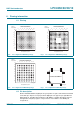
LPC4350/30/20/10 NXP Semiconductors 32-bit ARM Cortex-M4/M0 microcontroller offset error EO gain error EG 1023 1022 1021 1020 1019 1018 (2) 7 code out (1) 6 5 (5) 4 (4) 3 (3) 2 1 LSB (ideal) 1 0 1 2 3 4 5 6 7 1018 1019 1020 1021 1022 1023 1024 VIA (LSBideal) offset error EO 1 LSB = VDDA(3V3) − VSSA 1024 002aaf959 (1) Example of an actual transfer curve. (2) The ideal transfer curve. (3) Differential linearity error (ED). (4) Integral non-linearity (EL(adj)).
LPC4350/30/20/10 NXP Semiconductors 32-bit ARM Cortex-M4/M0 microcontroller Rvsi LPC43xx 2 kΩ (analog pin) 2.2 kΩ (multiplexed pin) ADC0_n/ADC1_n Rs ADC COMPARATOR Cia = 2 pF VEXT VSS 002aag704 Rs 1/((7 fclk(ADC) Cia) 2 k Fig 41. ADC interface to pins Table 35. DAC characteristics VDDA(3V3) over specified ranges; Tamb = 40 C to +85 C; unless otherwise specified Symbol ED Parameter Conditions differential linearity error 2.7 V VDDA(3V3) 3.6 V [1] 2.2 V VDDA(3V3) < 2.
LPC4350/30/20/10 NXP Semiconductors 32-bit ARM Cortex-M4/M0 microcontroller 13. Application information 13.1 LCD panel signal usage Table 36.
LPC4350/30/20/10 NXP Semiconductors 32-bit ARM Cortex-M4/M0 microcontroller Table 37.
LPC4350/30/20/10 NXP Semiconductors 32-bit ARM Cortex-M4/M0 microcontroller Table 38.
LPC4350/30/20/10 NXP Semiconductors 32-bit ARM Cortex-M4/M0 microcontroller Table 39. Recommended values for CX1/X2 in oscillation mode (crystal and external components parameters) low frequency mode …continued Fundamental oscillation frequency Maximum crystal series resistance RS External load capacitors CX1, CX2 12 MHz < 160 18 pF, 18 pF < 160 39 pF, 39 pF 16 MHz < 120 18 pF, 18 pF < 80 33 pF, 33 pF <100 18 pF, 18 pF < 80 33 pF, 33 pF 20 MHz Table 40.
LPC4350/30/20/10 NXP Semiconductors 32-bit ARM Cortex-M4/M0 microcontroller 13.3 RTC oscillator In the RTC oscillator circuit, only the crystal (XTAL) and the capacitances CRTCX1 and CRTCX2 need to be connected externally. Typical capacitance values for CRTCX1 and CRTCX2 are CRTCX1/2 = 20 (typical) 4 pF. An external clock can be connected to RTCX1 if RTCX2 is left open. The recommended amplitude of the clock signal is Vi(RMS) = 100 mV to 200 mV with a coupling capacitance of 5 pF to 10 pF.
LPC4350/30/20/10 NXP Semiconductors 32-bit ARM Cortex-M4/M0 microcontroller VDDIO ESD enable output driver data output from core PIN slew rate bit EHS input buffer enable bit EZI data input to core glitch filter filter select bit ZIF pull-up enable bit EPUN ESD pull-down enable bit EPD analog I/O VSSIO 002aah028 The glitch filter rejects pulses of typical 12 ns width. Fig 45. Standard I/O pin configuration with analog input 13.
LPC4350/30/20/10 NXP Semiconductors 32-bit ARM Cortex-M4/M0 microcontroller On the LPC4350/30/20/10, USBn_VBUS pins are 5 V tolerant only when VDDIO is applied and at operating voltage level. Therefore, if the USBn_VBUS function is connected to the USB connector and the device is self-powered, the USBn_VBUS pins must be protected for situations when VDDIO = 0 V. If VDDIO is always at operating level while VBUS = 5 V, the USBn_VBUS pin can be connected directly to the VBUS pin on the USB connector.
LPC4350/30/20/10 NXP Semiconductors 32-bit ARM Cortex-M4/M0 microcontroller LPC43xx VDDIO REGULATOR USBn_VBUS VBUS USB-B connector USB aaa-013459 Fig 48. USB interface on a bus-powered device Remark: If the VBUS function of the USB1 interface is not connected, configure the pin function for GPIO using the function control bits in the SYSCON block. VDDIO R1 LPC43xx T2 T1 R2 R3 USBn_VBUS VBUS USB-B connector USB aaa-013460 Fig 49.
LPC4350/30/20/10 NXP Semiconductors 32-bit ARM Cortex-M4/M0 microcontroller 14.
LPC4350/30/20/10 NXP Semiconductors 32-bit ARM Cortex-M4/M0 microcontroller TFBGA180: thin fine-pitch ball grid array package; 180 balls SOT570-3 A B D ball A1 index area E A2 A A1 detail X e1 e 1/2 e ∅v ∅w b M M C C A B C y y1 C P N M L K J H G F E D C B A ball A1 index area e e2 1/2 e 1 2 3 4 5 6 7 8 9 10 11 12 13 X 14 0 5 10 mm scale DIMENSIONS (mm are the original dimensions) UNIT mm max nom min A A1 A2 b D E e e1 e2 v w y y1 1.20 1.06 0.95 0.
LPC4350/30/20/10 NXP Semiconductors 32-bit ARM Cortex-M4/M0 microcontroller TFBGA100: plastic thin fine-pitch ball grid array package; 100 balls; body 9 x 9 x 0.7 mm B D SOT926-1 A ball A1 index area A2 E A A1 detail X e1 e ∅v ∅w b 1/2 e C M M C A B C y y1 C K J e H G F e2 E D 1/2 e C B A ball A1 index area 1 2 3 4 5 6 7 8 9 10 X 0 2.5 5 mm scale DIMENSIONS (mm are the original dimensions) UNIT A max A1 A2 b D E e e1 e2 v w y y1 mm 1.2 0.4 0.3 0.
LPC4350/30/20/10 NXP Semiconductors 32-bit ARM Cortex-M4/M0 microcontroller LQFP144: plastic low profile quad flat package; 144 leads; body 20 x 20 x 1.4 mm SOT486-1 c y X A 73 72 108 109 ZE e E HE A A2 (A 3) A1 θ wM Lp bp L pin 1 index detail X 37 144 1 36 v M A ZD wM bp e D B HD v M B 0 5 10 mm scale DIMENSIONS (mm are the original dimensions) UNIT A max. A1 A2 A3 bp c D (1) E (1) e mm 1.6 0.15 0.05 1.45 1.35 0.25 0.27 0.17 0.20 0.09 20.1 19.9 20.1 19.
LPC4350/30/20/10 NXP Semiconductors 32-bit ARM Cortex-M4/M0 microcontroller 15. Soldering Footprint information for reflow soldering of LBGA256 package SOT740-2 Hx P P Hy see detail X Generic footprint pattern Refer to the package outline drawing for actual layout solder land solder paste deposit solder land plus solder paste SL SP occupied area SR solder resist detail X DIMENSIONS in mm P SL SP SR 1.00 0.450 0.450 0.600 Hx Hy 17.500 17.500 sot740-2_fr Fig 54.
LPC4350/30/20/10 NXP Semiconductors 32-bit ARM Cortex-M4/M0 microcontroller Footprint information for reflow soldering of TFBGA180 package SOT570-3 Hx P P Hy see detail X Generic footprint pattern Refer to the package outline drawing for actual layout solder land solder paste deposit solder land plus solder paste SL SP occupied area SR solder resist detail X DIMENSIONS in mm P SL SP SR 0.80 0.400 0.400 0.550 Hx Hy 12.575 12.575 sot570-3_fr Fig 55.
LPC4350/30/20/10 NXP Semiconductors 32-bit ARM Cortex-M4/M0 microcontroller Footprint information for reflow soldering of LQFP144 package SOT486-1 Hx Gx P2 Hy (0.125) P1 Gy By Ay C D2 (8×) D1 Bx Ax Generic footprint pattern Refer to the package outline drawing for actual layout solder land occupied area DIMENSIONS in mm P1 0.500 P2 Ax Ay Bx By 0.560 23.300 23.300 20.300 20.300 C D1 D2 1.500 0.280 0.400 Gx Gy Hx Hy 20.500 20.500 23.550 23.550 sot486-1_fr Fig 56.
LPC4350/30/20/10 NXP Semiconductors 32-bit ARM Cortex-M4/M0 microcontroller Footprint information for reflow soldering of TFBGA100 package SOT926-1 Hx P P Hy see detail X Generic footprint pattern Refer to the package outline drawing for actual layout solder land solder paste deposit solder land plus solder paste SL SP occupied area SR solder resist detail X DIMENSIONS in mm P SL SP SR Hx Hy 0.80 0.330 0.400 0.480 9.400 9.400 sot926-1_fr Fig 57.
LPC4350/30/20/10 NXP Semiconductors 32-bit ARM Cortex-M4/M0 microcontroller 16. Abbreviations Table 41.
LPC4350/30/20/10 NXP Semiconductors 32-bit ARM Cortex-M4/M0 microcontroller 17. References LPC4350_30_20_10 Product data sheet [1] LPC43xx User manual UM10503: http://www.nxp.com/documents/user_manual/UM10503.pdf [2] LPC43X0 Errata sheet: http://www.nxp.com/documents/errata_sheet/ES_LPC43XX.pdf All information provided in this document is subject to legal disclaimers. Rev. 4.2 — 18 August 2014 © NXP Semiconductors N.V. 2014. All rights reserved.
LPC4350/30/20/10 NXP Semiconductors 32-bit ARM Cortex-M4/M0 microcontroller 18. Revision history Table 42. Revision history Document ID Release date Data sheet status LPC4350_30_20_10 v.4.2 20140818 Modifications: Change notice Supersedes Product data sheet LPC4350_30_20_10 v.4.1 • Parameter CI corrected for high-drive pins (changed from 2 pF to 5.2 pF). See Table 10. • • Table 18 “Dynamic characteristic: I/O pins[1]” added.
LPC4350/30/20/10 NXP Semiconductors 32-bit ARM Cortex-M4/M0 microcontroller Table 42. Revision history …continued Document ID LPC4350_30_20_10 v.3.7 Modifications: LPC4350_30_20_10 v.3.6 Modifications: LPC4350_30_20_10 v.3.5 LPC4350_30_20_10 Product data sheet Release date Data sheet status Change notice Supersedes • Parameter ILH (High-level leakage current) for condition VI = 5 V changed to 20 nA (max). See Table 10.
LPC4350/30/20/10 NXP Semiconductors 32-bit ARM Cortex-M4/M0 microcontroller Table 42. Revision history …continued Document ID Modifications: Release date Data sheet status Change notice Supersedes • Temperature range for simulated timing characteristics corrected to Tamb = 40 C to +85 C in Section 11 “Dynamic characteristics”. • • • • • • SPIFI timing added. See Section 11.15. SPIFI maximum data rate changed to 52 MB per second. Editorial updates.
LPC4350/30/20/10 NXP Semiconductors 32-bit ARM Cortex-M4/M0 microcontroller 19. Legal information 19.1 Data sheet status Document status[1][2] Product status[3] Definition Objective [short] data sheet Development This document contains data from the objective specification for product development. Preliminary [short] data sheet Qualification This document contains data from the preliminary specification. Product [short] data sheet Production This document contains the product specification.
LPC4350/30/20/10 NXP Semiconductors 32-bit ARM Cortex-M4/M0 microcontroller Export control — This document as well as the item(s) described herein may be subject to export control regulations. Export might require a prior authorization from competent authorities. Non-automotive qualified products — Unless this data sheet expressly states that this specific NXP Semiconductors product is automotive qualified, the product is not suitable for automotive use.
LPC4350/30/20/10 NXP Semiconductors 32-bit ARM Cortex-M4/M0 microcontroller 21. Contents 1 2 3 4 4.1 5 6 6.1 6.2 7 7.1 7.2 7.3 7.4 7.5 7.6 7.6.1 7.6.2 7.7 7.8 7.9 7.9.1 7.10 7.11 7.12 7.13 7.14 7.15 7.15.1 7.16 7.16.1 General description . . . . . . . . . . . . . . . . . . . . . . 1 Features and benefits . . . . . . . . . . . . . . . . . . . . 1 Applications . . . . . . . . . . . . . . . . . . . . . . . . . . . . 4 Ordering information . . . . . . . . . . . . . . . . . . . . . 5 Ordering options . . . .
LPC4350/30/20/10 NXP Semiconductors 32-bit ARM Cortex-M4/M0 microcontroller 7.22.6 7.22.7 7.22.8 7.22.9 7.22.10 7.23 8 9 10 10.1 10.2 10.3 10.4 11 11.1 11.2 11.3 11.4 11.5 11.6 11.7 11.8 11.9 11.10 11.11 11.12 11.13 11.14 11.15 11.16 11.17 11.18 11.19 12 13 13.1 13.2 13.3 13.4 13.5 13.6 13.7 14 15 16 17 18 PLL0AUDIO (for audio) . . . . . . . . . . . . . . . . . 82 System PLL1 . . . . . . . . . . . . . . . . . . . . . . . . . 82 Reset Generation Unit (RGU). . . . . . . . . . . . . 82 Power control . . .