
Datasheet


LPC4350_30_20_10 All information provided in this document is subject to legal disclaimers. © NXP Semiconductors N.V. 2014. All rights reserved.
Product data sheet Rev. 4.2 — 18 August 2014 10 of 155
NXP Semiconductors
LPC4350/30/20/10
32-bit ARM Cortex-M4/M0 microcontroller
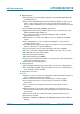
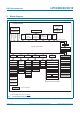
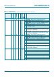
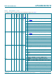
P1_1 R2 N1 K2 42
[2]
N;
PU
I/O GPIO0[8] — General purpose digital input/output pin. Boot pin
(see Table 5).
O CTOUT_7 — SCTimer/PWM output 7. Match output 3 of timer
1.
I/O EMC_A6 — External memory address line 6.
I/O SGPIO8 — General purpose digital input/output pin.
- R — Function reserved.
I/O SSP0_MISO — Master In Slave Out for SSP0.
- R — Function reserved.
- R — Function reserved.
P1_2 R3 N2 K1 43
[2]
N;
PU
I/O GPIO0[9] — General purpose digital input/output pin. Boot pin
(see Table 5
).
O CTOUT_6 — SCTimer/PWM output 6. Match output 2 of timer
1.
I/O EMC_A7 — External memory address line 7.
I/O SGPIO9 — General purpose digital input/output pin.
- R — Function reserved.
I/O SSP0_MOSI — Master Out Slave in for SSP0.
- R — Function reserved.
- R — Function reserved.
P1_3 P5 M2 J1 44
[2]
N;
PU
I/O GPIO0[10] — General purpose digital input/output pin.
O CTOUT_8 — SCTimer/PWM output 8. Match output 0 of timer
2.
I/O SGPIO10 — General purpose digital input/output pin.
O EMC_OE
— LOW active Output Enable signal.
O USB0_IND1 — USB0 port indicator LED control
output 1.
I/O SSP1_MISO — Master In Slave Out for SSP1.
- R — Function reserved.
O SD_RST — SD/MMC reset signal for MMC4.4 card.
P1_4 T3 P2 J2 47
[2]
N;
PU
I/O GPIO0[11] — General purpose digital input/output pin.
O CTOUT_9 — SCTimer/PWM output 9. Match output 3 of timer
3.
I/O SGPIO11 — General purpose digital input/output pin.
O EMC_BLS0
— LOW active Byte Lane select signal 0.
O USB0_IND0 — USB0 port indicator LED control output 0.
I/O SSP1_MOSI — Master Out Slave in for SSP1.
- R — Function reserved.
O SD_VOLT1 — SD/MMC bus voltage select output 1.
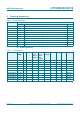
Table 3. Pin description
…continued
LCD, Ethernet, USB0, and USB1 functions are not available on all parts. See Table 2.
Symbol
LBGA256
TFBGA180
TFBGA100
LQFP144
Reset state
[1]
Type
Description