
Datasheet


LPC4350_30_20_10 All information provided in this document is subject to legal disclaimers. © NXP Semiconductors N.V. 2014. All rights reserved.
Product data sheet Rev. 4.2 — 18 August 2014 7 of 155
NXP Semiconductors
LPC4350/30/20/10
32-bit ARM Cortex-M4/M0 microcontroller
6. Pinning information
6.1 Pinning
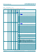
6.2 Pin description
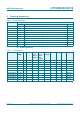
On the LPC4350/30/20/10, digital pins are grouped into 16 ports, named P0 to P9 and PA
to PF, with up to 20 pins used per port. Each digital pin can support up to eight different
digital functions, including General-Purpose I/O (GPIO), selectable through the System
Configuration Unit (SCU) registers. The pin name is not indicative of the GPIO port
assigned to it.
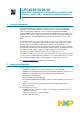
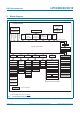
Fig 2. Pin configuration LBGA256 package Fig 3. Pin configuration TFBGA180 package
002aaf813
LPC4350/30FET256
Transparent top view
T
R
P
N
M
L
J
G
K
H
F
E
D
C
B
A
2 4 6 8 10 12
13
14
15
16
1357911
ball A1
index area
002aag374
LPC4350/30FET180
Transparent top view
N
L
P
M
K
J
H
G
F
D
B
E
C
A
2 4 6 8 10 12
13
14
1357911
ball A1
index area
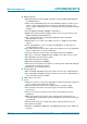
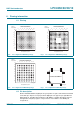
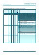
Fig 4. Pin configuration TFBGA100 package Fig 5. Pin configuration LQFP144 package
002aag375
LPC4330/20/10FET100
Transparent top view
J
G
K
H
F
E
D
C
B
A
24681013579
ball A1
index area
LPC4330/20/10FBD144
72
1
36
108
73
37
109
144
002aag377