
Datasheet

LPC4350_30_20_10 All information provided in this document is subject to legal disclaimers. © NXP Semiconductors N.V. 2014. All rights reserved.
Product data sheet Rev. 4.2 — 18 August 2014 9 of 155
NXP Semiconductors
LPC4350/30/20/10
32-bit ARM Cortex-M4/M0 microcontroller
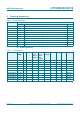
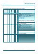
Table 3. Pin description
LCD, Ethernet, USB0, and USB1 functions are not available on all parts. See Table 2.
Symbol
LBGA256
TFBGA180
TFBGA100
LQFP144
Reset state
[1]
Type
Description
Multiplexed digital pins
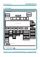
P0_0 L3 K3 G2 32
[2]
N;
PU
I/O GPIO0[0] — General purpose digital input/output pin.
I/O SSP1_MISO — Master In Slave Out for SSP1.
I ENET_RXD1 — Ethernet receive data 1 (RMII/MII interface).
I/O SGPIO0 — General purpose digital input/output pin.
- R — Function reserved.
- R — Function reserved.
I/O I2S0_TX_WS — Transmit Word Select. It is driven by the
master and received by the slave. Corresponds to the signal
WS in the I
2
S-bus specification.
I/O I2S1_TX_WS — Transmit Word Select. It is driven by the
master and received by the slave. Corresponds to the signal
WS in the I
2
S-bus specification.
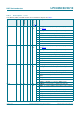
P0_1 M2 K2 G1 34
[2]
N;
PU
I/O GPIO0[1] — General purpose digital input/output pin.
I/O SSP1_MOSI — Master Out Slave in for SSP1.
I ENET_COL — Ethernet Collision detect (MII interface).
I/O SGPIO1 — General purpose digital input/output pin.
- R — Function reserved.
- R — Function reserved.
ENET_TX_EN — Ethernet transmit enable (RMII/MII
interface).
I/O I2S1_TX_SDA — I2S1 transmit data. It is driven by the
transmitter and read by the receiver. Corresponds to the signal
SD in the I
2
S-bus specification.
P1_0 P2 L1 H1 38
[2]
N;
PU
I/O GPIO0[4] — General purpose digital input/output pin.
I CTIN_3 — SCTimer/PWM input 3. Capture input 1 of timer 1.
I/O EMC_A5 — External memory address line 5.
- R — Function reserved.
- R — Function reserved.
I/O SSP0_SSEL — Slave Select for SSP0.
I/O SGPIO7 — General purpose digital input/output pin.
- R — Function reserved.